


Underneath the main chassis we could see left and right were two substantial plastic side rails. Also underneath were two grooved bars, theses bars are pivoted on one end. These are swung left and right which unlocks the two plastic side rails. Then gently lift from the front and the side rails slip into the rails allowing the whole chassis to be extended out from the set by about a 25cm, this now gives plenty of clearance front, back and sides.


The two upright side panels have a locking hinge bar, when this is unlatched each panel can be swung down to a horizontal service position. Finally the Line stage cage can be hinged up giving access to the the components within. All in all superb access is afforded to the service engineer.


The TELEFUNKEN CHASSIS 712 is introducing the 20AX CRT TUBE TECHNOLOGY WITH INLINE GUN TYPE (PHILIPS).


-
-


Synchronization BS531 AT349354014 with ITT TBA950X2
- Frame Oscillator BS451 AT349354015
- Frame deflection output amplifier BS491 AT349354016 with BD312T + 2N5877T
(Motorola + Fairchild)
- E/W Correction unit BS AT349354017
- CHROMA I (LUMINANCE) AT349354009 BS301
- CHROMA II (CHROM + MATRIX) AT349354010 BS201
- NETZTEIL BS401 AT349354
- NETZTEIL 2 BS421
- LINE DEFLECTION BS561
- SOUND (TON) BS151 AT349354008 BS151
- RGB ENDSTUFE (RGB AMPL) AT349354021 BS332 BS331
TELEFUNKEN PALCOLOR 746 CHASSIS 712 Tuning circuit arrangement:
A tuning circuit arrangement comprises one or more tuned circuits whose frequency range is tuned by tuning diodes, means being provided for varying the tuning voltage of the tuning diodes to provide exclusive variation of the tuned circuit capacitance of the tuned circuit.

 1. A circuit for adjusting a tuning circuit, the tuning circuit including at least one resonant circuit composed of a variable inductance and a variable capacitance constituted by at least one voltage-variable tuning diode, one side of the resonant circuit being connected to a point at circuit ground potential and adjustment of the resonant circuit being effected by changing the resonant circuit inductance and the resonant circuit capacitance, with changing of the resonant circuit capacitance being effected exclusively by varying the tuning voltage of the tuning diode, the tuning circuit further including a source of a variable tuning potential which is variable over a range between maximum and minimum extreme values, each extreme value being different from the circuit ground potential, and said circuit for adjusting comprising at least one adjustment potentiometer connected between a point of said source providing the variable tuning potential and a point of said source permanently providing one of said extreme values, said potentiometer having an adjustable tap connected to provide the tuning voltage for said tuning diode. 2. An arrangement as defined in claim 1 wherein said tuning circuit includes a plurality of said resonant circuits and said circuit for adjusting comprises a plurality of said potentiometers connected together in parallel and each having a respective adjustable tap connected to provide the tuning voltage for at least one respective tuning diode. 3. An arrangement as defined in claim 1 wherein said source comprises a tuning potentiometer connected to have a respective one of the extreme values of the tuning potential at each of its ends and having an adjustable tap providing the variable tuning potential, and said adjustment potentiometer is connected between one end and said movable tap of said tuning potentiometer. 4. An arrangement as defined in claim 1 wherein said tuning circuit includes at least two of said resonant circuits and said adjustable tap of said adjustment potentiometer is connected to provide the tuning voltage for said at least two resonant circuits. 5. An arrangement as defined in claim 4 wherein said resonant circuits have respectively different relative frequency variations.
 1. A circuit for adjusting a tuning circuit, the tuning circuit including at least one resonant circuit composed of a variable inductance and a variable capacitance constituted by at least one voltage-variable tuning diode, one side of the resonant circuit being connected to a point at circuit ground potential and adjustment of the resonant circuit being effected by changing the resonant circuit inductance and the resonant circuit capacitance, with changing of the resonant circuit capacitance being effected exclusively by varying the tuning voltage of the tuning diode, the tuning circuit further including a source of a variable tuning potential which is variable over a range between maximum and minimum extreme values, each extreme value being different from the circuit ground potential, and said circuit for adjusting comprising at least one adjustment potentiometer connected between a point of said source providing the variable tuning potential and a point of said source permanently providing one of said extreme values, said potentiometer having an adjustable tap connected to provide the tuning voltage for said tuning diode. 2. An arrangement as defined in claim 1 wherein said tuning circuit includes a plurality of said resonant circuits and said circuit for adjusting comprises a plurality of said potentiometers connected together in parallel and each having a respective adjustable tap connected to provide the tuning voltage for at least one respective tuning diode. 3. An arrangement as defined in claim 1 wherein said source comprises a tuning potentiometer connected to have a respective one of the extreme values of the tuning potential at each of its ends and having an adjustable tap providing the variable tuning potential, and said adjustment potentiometer is connected between one end and said movable tap of said tuning potentiometer. 4. An arrangement as defined in claim 1 wherein said tuning circuit includes at least two of said resonant circuits and said adjustable tap of said adjustment potentiometer is connected to provide the tuning voltage for said at least two resonant circuits. 5. An arrangement as defined in claim 4 wherein said resonant circuits have respectively different relative frequency variations.
Description:
BACKGROUND OF THE INVENTION
The invention relates to a tuning circuit arrangement comprising one or more tuning circuits in which tuning diodes are provided for tuning of the frequency range. In such an arrangement, the adjustment of the tuned circuit takes place, for example, by changing the tuned circuit inductance and the tuned circuit capacitance.
As is known, tuning circuits have the object of tuning the resonant circuits of selective amplifiers and/or oscillators to a given resonant frequency. In a known tuning circuit, the adjustment to synchronous operation in each circuit takes place via a tuning coil and a particular trimmer capacitor. In the known tuning circuit arrangement a multiply repeated adjustment of the inductance and the capacitance is required for adjustment to synchronous operation, because the setting of the trimmer capacitors again changes the resonant frequency of the frequency previously set inductively.
SUMMARY OF THE INVENTION
It is an object of the invention to provide a tuning circuit arrangement with simplified adjustment.
According to a first aspect of the invention, there is provided a tuning circuit arrangement comprising one or more tuned circuits, tuning diodes in said tuned circuits for tuning the frequency range of said tuned circuits and means for varying the tuning voltage of said tuning diodes for providing exclusive variation of the tuned circuit capacitance of said tuned circuit.
According to a second aspect of the invention, there is provided a tuning circuit arrangement comprising one or more tuning circuits, in which tuning diodes are provided for the purpose of tuning the frequency range and in which the tuned circuit adjustment takes place by changing the tuned circuit inductance and the tuned circuit capacitance, characterized in that the adjustment in capacitance takes place exclusively by varying the tuning voltage for the tuning diode(s).
BRIEF DESCRIPTION OF THE DRAWINGS
The invention will now be described in greater detail, by way of example, with reference to the drawings in which:
FIG. 1 is a circuit diagram showing a first form of circuit arrangement in accordance with the invention as applied to two resonant circuits;
FIG. 2 is a circuit diagram similar to FIG. 1 but showing the arrangement applied to n resonant circuits;
FIG. 3 is a circuit diagram similar to FIG. 1 but showing the arrangement with a different form of adjustment;
FIG. 4 is a circuit diagram similar to FIG. 2 in which the arrangement of FIG. 3 is applied to n resonant circuits;
FIG. 5 is a circuit diagram showing a part of the arrangement showing a different form of adjusting circuitry;
FIG. 6 is a circuit diagram similar to FIG. 5 but showing a still further form of adjusting circuitry;
FIG. 7 is a block diagram of part of the arrangement provided with temperature compensation and,
FIG. 8 is a block diagram similar to FIG. 7 but including a decoupling circuit.
DESCRIPTION OF THE PREFERRED EMBODIMENTS
In a tuning circuit arrangement of the type mentioned at the beginning it is proposed in accord ance with the invention and in order to solve the object that the adjustment in capacitance should take place exclusively by variation of the tuning voltage for the tuning diode(s).
 ance with the invention and in order to solve the object that the adjustment in capacitance should take place exclusively by variation of the tuning voltage for the tuning diode(s).
The essence of the invention on the one hand consists in that special trimmer capacitors for achieving an adjustment in capacitance are omitted and that the adjustment in capacitance takes place exclusively by variations of the tuning voltage for the tuning diode(s) which is in contrast to the known method, and does not take place by means of trimmer capacitors. On the other hand, the invention does not require any repetitive adjustment of the tuned circuits of the tuning circuits.
The tuning circuit arrangement in accordance with the invention makes it possible to reduce considerably the required maximum tuning voltage. With the tuning circuit arrangement in accordance with the invention it is possible to operate with small tuning voltages even when using tuning diodes having abrupt pn junction. The sought after simplification of the adjustment can be achieved by means of the fact that the capacitative adjustment does not influence the previously operated adjustment in inductance.
In the tuning circuit arrangement according to the invention potentiometers, for example, are provided in order to adjust the capacitance. There is the possibility of using the same adjusting means for adjusting the capacitance of two or more tuned circuits. Similarly, the same adjustment means may serve to adjust the capacitance of several tuned circuits having varying relative frequency variation.
In accordance with a further refinement of the invention a circuit arrangement for producing minimum and maximum tuning potentials is provided which is constructed so that the potentials produced by it have such a temperature dependence that the effect of temperature on the tuning circuit is compensated.
It is advisable to connect a decoupling circuit between the means for adjusting capacitance and the 6 tuning potentiometers, the decoupling circuit reducing the electrical load on the tuning potentiometer through the adjustment means. In accordance with an embodiment of the invention, precautions are taken to ensure that one of the two potentials applied to an adjustment potentiometer, does not change during adjustment.
The adjustment potentiometer or potentiometers are connected for example between a point in the circuit at which the variable tuning potential is available and a point in the circuit at which the minimum tuning potential is available. There is also the possibility of connecting the adjustment potentiometer or potentiometers between a point in the circuit at which the variable tuning potential is available and a point in the circuit at which the maximum tuning potential is available.
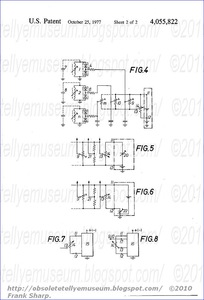
Referring now to the drawings, FIG. 1 shows an electronic tuning circuit in accordance with the inv ention which operates with tuning diodes. The tuning circuit of FIG. 1, which is for example a component of a VHF tuner, consists of two variable-frequency resonant circuits and in fact an oscillator circuit 1 and a resonant circuit 2 for selecting the input signal. The oscillator circuit comprises an inductance 3 and a tuning diode 4, which is a double diode in this embodiment. The resonant circuit 2 comprises an inductance 5 and a tuning diode 6, which in this embodiment is also a double diode. As may be seen from FIG. 1, neither of the two resonant circuits 1 and 2 has a trimmer capacitor. Of course, parallel to the resonant circuits there are unavoidable circuit capacitances 7 and 8 which are shown in broken lines.
 ention which operates with tuning diodes. The tuning circuit of FIG. 1, which is for example a component of a VHF tuner, consists of two variable-frequency resonant circuits and in fact an oscillator circuit 1 and a resonant circuit 2 for selecting the input signal. The oscillator circuit comprises an inductance 3 and a tuning diode 4, which is a double diode in this embodiment. The resonant circuit 2 comprises an inductance 5 and a tuning diode 6, which in this embodiment is also a double diode. As may be seen from FIG. 1, neither of the two resonant circuits 1 and 2 has a trimmer capacitor. Of course, parallel to the resonant circuits there are unavoidable circuit capacitances 7 and 8 which are shown in broken lines.
The two resonant circuits 1 and 2 must be adjusted to achieve synchronous operation. In accordance with the invention the adjustment potentiometers 9 and 10 are provided for this purpose. The adjustment potentiometers 9 and 10 are connected in parallel with one another in the embodiment of FIG. 1. Two limiting potentials are required for the tuning circuit; in fact the largest potential U max at point 11 and the smallest potential U min at point 12. In the embodiment of FIG. 1 the two adjustment potentiometers 9 and 10 lie between the wiper contact 13 of the tuning potentiometer 14 and the point 12 having the potential U min . The tuning potentiometer 14 lies between the points 11 and 12, i.e. between the maximum potential U max and the minimum potential U min . The maximum tuning potential U max and the minimum tuning potential U min are in fact linked together, yet they are produced in a separate circuit arrangement. This is indicated symbolically in FIG. 1 by means of the two voltage sources 23 and 24. The minimum tuning potential U min is therefore not derived via a purely ohmic voltage divider from the maximum tuning potential U max .
In the tuning circuit of FIG. 1, in the case where the tuning potentiometer 14 is set to the minimum tuning voltage, the voltages taken from the adjustment potentiometers 9 and 10 are not influenced by the settings of the adjustment potentiometer. Therefore, if the wiper contact 13 of the tuning potentiometer 14 is located at the lowest position then no matter how the adjustment potentiometers 9 and 10 are rotated the adjustment voltages for the tuning diodes will not be influenced by this. This has the consequence that setting in the upper frequency range has no influence on the previously set lower frequency. The adjustment of the lower frequency is only dependent on the inductance adjustment of the inductances 3 and 5.
The tuning circuit of FIG. 2 is distinguished from the tuning circuit of FIG. 1 by the fact that instead of only two resonant circuits n resonant circuits are provided and, instead of only two adjustment potentiometers, m adjustment potentiometers are provided. m may be smaller than n if not merely one resonant circuit but more than one resonant circuit is adjusted by means of a single adjustment potentiometer.
FIG. 3 shows an embodiment of the invention in which in contrast to FIGS. 1 and 2 the adjustment potentiometers 9 and 10 lie between the wiper contact 13 of the tuning potentiometer 14 and point 11 having the potential U max . In this case, the adjustment in inductance takes place in the upper frequency and the adjustment in capacitance takes place in the lower frequency by means of the adjustment potentiometers 9 and 10.
The tuning circuit of FIG. 4 is distinguished from the tuning circuit of FIG. 3 by the fact that, instead of only two resonant circuits, again n resonant circuits are provided and instead of only two adjustment potentiometers m adjustment potentiometers are provided.
According to FIG. 5 the adjustment in capacitance is undertaken for the upper frequency by setting the maximum tuning potential. While in the tuning circuits of FIGS. 1 to 4 the adjustment of the individual tuned circuits is independent, in the arrangement of FIG. 5 the setting of the maximum tuning potential effects all tuned circuits. The setting of the maximum tuning potential takes place in the arrangement of FIG. 5 by means of the voltage source 20. The voltage supplying the tuning diodes may for example be taken from the wiper contact 13 of the tuning potentiometer 14, from a fixed voltage divider 21 or from the wiper contact of the adjustment potentiometer 9. Several adjustment potentiometers may be provided instead of only one adjustment potentiometer.
The arrangement of FIG. 6 is distinguished from the arrangement of FIG. 5 by the fact that the minimum tuning potential is made settable instead of the maximum tuning potential for the purpose of adjustment. Moreover, in the arrangement of FIG. 6, the network which comprises the voltage divider 21 and the adjustment potentiometer 9, is connected between the wiper contact 13 of the adjustment potentiometer 14 and the maximum tuning potential 11.
According to FIG. 7, the maximum and minimum tuning potential is produced by means of a circuit arrangement 15 which has the object of supplying such a temperature effect of the potential that the temperature effect of the tuning circuit is compensated by an appropriate temperature effect of the potentials.
The arrangement 16 of FIG. 8 also produces the minimum and maximum tuning potentials at the points 11 and 12 as well as the effective temperature on these potentials which is required for temperature compensation of the tuning circuit. In addition, the arrangement 16 contains a decoupling circuit which lies between the wiper contact 13 of the tuning potentiometer 14 and the adjustment potentiometers 9 and 10.
The tuning circuit dealt with in the embodiments is developed for positive tuning potentials. In a similar manner, the tuning circuits of the invention may also be designed for negative tuning potentials.
It will be understood that the above description of the present invention is susceptible to various modification changes and adaptations.
TELEFUNKEN PALCOLOR 746 CHASSIS 712 20AX power supply CONSTANT-VOLTAGE CONVERTER EMPLOYING THYRISTOR:
 In a television receiver for the consumer market it is desirable to provide an economical unit with optimum operating reliability. With the advent of semiconductor devices many significant contributions both in device and circuit technology, have resulted in the wide spread application of such devices in the television receiver environment. In the transition from vacuum tube receivers to those receivers employing semiconductor devices, as transistors, the designer encountered specific problems due to the dissimilarity between such devices.
For example, in the field of power supply design, vacuum tubes require substantially higher operating voltages than most readily available transistors. Due to the power supply requirements of vacuum tubes it was relatively simple to design a television receiver for direct AC line operation. Such a receiver employing vacuum tubes could be operated directly from the AC lines, if so desired, without the inclusion of a separate power transformer. This technique was especially advantageous in European receivers where the AC line potential is on the order of magnitude of 220 volts. Therefore, by direct rectification the DC potentials produced are perfectly compatible with the vacuum tube devices. Accordingly, many European and domestic manufacturers, as well, marketed television receivers without utilizing the relatively expensive power transformer. With such a background in mind, and the increased availability of transistors, those manufacturers would still desire to produce a television receiver for direct AC line operation and thereby avoid using an expensive power transformer. However, as indicated above, the operating potentials required for transistor operation are not easily obtainable directly from the AC line. There are prior art circuit techniques for reducing the effective potential from the AC line as applied, for example, to a television receiver. Such techniques, however, dissipate excessive power and are limited in their regulation and current handling capabilities. Furthermore, coupled with the expanding semiconductor technology is the expanding utilization of color television transmission and receiving equipment.
 Power supply design for color television receivers dictates stringent requirements for the functional and overall characteristics of the power supplies to be utilized therein.
Essentially the power supplies to be utilized in a color television receiver should preferably be well regulated against transients and varying voltage conditions which can and do occur on the AC lines. Such supplies should be regulated against varying load conditions which can occur within the television receiver itself. Furthermore, the operation of these supplies must be such that harmonic generation therein is well discriminated against so as to avoid stray coupling back to the high gain radio frequency or intermediate frequency amplifying stages.
A further desire in a television receiver is to provide a high voltage supply for operating the kinescope. Such a supply should be capable of providing a relatively high potential ultor voltage which is regulated according to AC line voltage and load current variations. This action results in a relatively constant raster size which is independent of AC line voltage and kinescope beam current variations.
When such supplies are operating in consumer equipments, as television receivers, one has to consider the wide spread distribution of such receivers and the operation of such receivers as affecting the power handling capability of the power companies. With regard to semiconductor devices, in general, as utilized in power supply equipment, a device which has found wide spread use for such application is the thyristor or the silicon controlled rectifier device. Such devices are basically phase controlled rectifiers whereby the conduction of the device can be made to depend upon a voltage applied to a control electrode referred to as the gate.
 Many applications of controlled or switched rectifiers such as thyristors can be found in the prior art. Such prior art is concerned with protection circuits to allow these semiconductor devices to operate with reactive loads, or under varying line conditions, or under varying load conditions. The nature of such uses depends largely upon the specific application or environment in which the device is employed. However, it will be apparent that none of the prior art techniques serve to solve the many and peculiar problems faced in the operation and environment of a television receiver.
It is therefore an object of the present invention to provide improved thyristor power supply circuits for direct operation from AC line in economical and reliable configurations.
A further object is to provide a thyristor supply employing regulation and capable of providing a high operating potential for a kinescope.
According to a feature of the present invention, a thyristor is employed in a power supply configuration connected directly across the AC lines. The thyristor has the gate electrode coupled to a transistor circuit used for controlling the conduction angle of the thyristor, for regulation of the supply voltage. The base electrode of the transistor gate is provided with signals proportional to both the AC line voltage and the DC output voltage of the supply. The thyristor supply is also used to provide B+ for a horizontal output stage. The output transformer which is coupled to the horizontal output stage provides a stepped-up voltage which is rectified to produce the high voltage necessary to operate the ultor of the kinescope. The regulation provided to the thyristor is dependent upon the internal impedance of the power supply which is determined by the feedback used to provide the transistor with the voltage proportional to the DC output voltage. Regulation is affected by kinescope beam current, and is also dependent on line voltage variations, both of which operate to serve to provide a relatively constant raster size substantially independent of such variations.
A constant voltage converter having a rectifier for rectifying AC power and with a thyristor connected between the rectifier and a filter for selectively passing therethrough a rectified output to an output terminal. There is a wave generator connected to the output of the rectifier for producing a first signal and an intergrator circuit connected to the output of the wave generator for producing an integral output in response to this first signal. In addition there is a detector circuit for detecting a fluctuation of the rectified output power and for producing second signal. A comparison circuit is connected between the intergrator circuit and the detector circuit for producing third signal in accordance with the comparison. A trigger circuit is connected between the comparison circuit and the control gate of the thyristor for supplying a phase control signal to the thyristor to thereby obtain a constant voltage output regardless of the fluctuation of the rectified output.
1. A
 constant voltage converter comprising an input of a power supply means, an output terminal, filter means, rectifier means connected to said input for rectifying a.c. power and for supplying output thereof to said output terminal, thyristor means connected between said rectifier means and said filter means for selectively passing therethrough a rectified output to the output terminal by way of said filter means, saw-tooth wave generator means connected between the output of said rectifier means and at least one integrator circuit means for producing an integral output in response to a saw-tooth wave produced, a first transistor in said saw-tooth wave generator, the input of said integrator circuit means being connected to a collector of said first transistor, detector circuit means connected to said output terminal for detecting a fluctuation of the rectified output power and for producing an output signal, said detector circuit means having a second transistor, pulse generator circuit means connected between said saw-tooth wave generator means and said detector circuit means for producing a trigger pulse to said thyristor through a trigger means, a third transistor in said pulse circuit generator means, the base of said third transistor being connected to the output of said integrator circuit means, the emitter thereof being connected to the emitter of said second transistor in said detector circuit means, and the collector thereof being connected to the gate of the thyristor means so as to supply a phase control signal thereto, thereby obtaining a constant voltage output regardless of the fluctuation of the rectified output.
 Description:
This invention relates to constant-voltage converters and more particularly to a constant-voltage converter employing a thyristor.
Description:
This invention relates to constant-voltage converters and more particularly to a constant-voltage converter employing a thyristor.
Conventional constant-voltage converters of the type employing a thyristor are arranged to phase shift and full-wave-rectify an input a.c. power applied thereto and to maintain the output voltages constant by regulating the firing angle of the thyristor in comparison of the output voltages with the phase-shifted and rectified input a.c. power. When, however, these converters are connected to a common a.c. source having a relatively high internal impedance, the waveform of the phase-shifted and rectified a.c. input power is distorted thereby causing undesired operations of the converters.
It is therefore an object of the present invention to provide a constant-voltage converter which correctly operates notwithstanding the distortion of the input a.c. voltage.
Another object of the invention is to provide a constant-voltage converter which effectively suppress an undesired rush current.
Another object of the invention is to provide a constant-voltage converter having an improved feed-back circuit of a substantially constant loop gain .
In the drawings:
FIG. 1 is a schematic view of a converter according to the present invention;
FIG. 2 is a diagram showing a circuit arrangement of the converter of FIG. 1;
FIG. 3 is a diagram showing various waveforms of signals appearing in the circuit of FIG. 2;
FIG. 4 is a diagram showing various waveforms appearing in the circuit of FIG. 2 when an a.c. power is supplied to the circuit;
FIG. 5 is a diagram showing another circuit arrangement of the converter of FIG. 1;
FIG. 6 is a diagram showing waveforms of signals appearing in the circuit of FIG. 5; and
FIG. 7 is a diagram showing further another circuit arrangement of generator the of FIG. 1.
Referring now to FIG. 1, a cons tant-voltage converter 10 according to the present invention comprises a rectifier 11 having two input terminals 12 and 13 through which an a.c. power is supplied. The rectifier 11 is preferably a full-wave rectifier although a half-wave rectifier may be employed. An output 14 of the rectifier 11 is connected through a line 15 to an anode of a thyristor 16. The thyristor 16 passes therethrough the rectified a.c. power in only one direction from its anode to cathode when triggered by a trigger pulse through its gate. The cathode of the thyristor 16 is connected through a line 17 to an input of a smoothing filter 18. The smoothing filter 18 smoothes the power from the thyristor 16. An output of the smoothing filter 18 is connected through a line 19 to an output terminal 20. The output 14 of the rectifier 11 is also connected through a line 21 to a saw-tooth wave generator 22 which generates a saw-tooth wave signal having the same repetition period as the rectified input a.c. power. An output of the saw-tooth wave generator 22 is connected through a line 23 to one input of a trigger pulse generator 24. The other input of the trigger pulse generator 24 is connected through a line 25 to the line 19. An output of the trigger pulse generator 24 is connected through a line 26 to the gate of the thyristor 16. The trigger pulse generator 24 produces a trigger pulse on its output when the voltage of the saw-tooth wave signal reaches a level which is varied in response to the output voltage on the terminal 20. The trigger pulse generator 24 may be variously arranged and in this case arranged to comprise rectangular generator 27 having one input connected through the line 23 to the saw-tooth wave generator 22 and the other input connected through a line 28 to an output voltage detector 29. The detector 29 produces a reference signal representing the output voltage on the terminal 20. The pulse generator 27 is adapted to produces a rectangular pulse when the saw-tooth wave signal to the one input reaches a level which defined is in accordance with the reference signal. An output of the rectangular pulse generator 27 is connected through a line 30 to an input of a trigger circuit 31. The trigger circuit 31 is adapted to convert the rectangular pulse into a spike pulse. An output of the trigger circuit 31 is connected through the line 26 to the gate of the thyristor 16.
FIG. 2 illustrates a prefe rred circuit arrangement of the converter shown in FIG. 1 which comprises a rectifier 11 of a full-wave rectifier consisting of rectifiers 40, 41, 42 and 43. Inputs of the rectifier are connected to terminals 12 and 13 through which an a.c. power is applied. The output 14 of the rectifier 11 is connected through a line 15 to an anode of a thyristor 16. A cathode of the thyristor 16 is connected through a line 17 to a smoothing filter 18 which includes a capacitor C4 having one terminal connected to the line 17 and the other terminal grounded. The output of the smoothing filter 18 is connected through a line 19 to an output terminal 20.
The saw-tooth wave generator 22 includes a resistor R 1 having one terminal connected to the line 21 and the terminal connected through a junction J 1 to one terminal of a resistor R 2 . The other terminal of the resistor R 2 is grounded. The junction J 1 is connected through a coupling capacitor C 1 to a base of a transistor T 1 of PNP type. An emitter of the transistor T 1 is connected through a resistor R 3 to the line 21. A resistor R 4 is provided between the emitter and the base of the transistor T 1 so as to apply a bias potential to the base. A collector of the transistor T 1 is grounded through a parallel connection of a resistor R 5 and capacitor C 2 . To the emitter is connected a capacitor C 3 which is in turn grounded and passes therethrough only a.c. signals to the ground.
The rectangular pulse generator 27 comprises a transistor T 2 of PNP type having a base connected through a resistor R 6 to the collector of the transistor T 1 . An emitter of the transistor T 2 is connected through a resistor R 7 to the emitter of the transistor T 1 . A collector of the transistor T 2 is grounded through a resistor R 8 and connected through the line 30 to one terminal of a capacitor C 4 of the trigger circuit 31. The other terminal of the capacitor C 4 is connected through a line 26 to the gate of the thyristor 16.
The output voltage detector 29 includes a transistor T 3 of NPN type having an emitter grounded through a zener diode ZD. A collector of the transistor T 3 is connected through a line 28 to the emitter of the transistor T 2 and, on the other hand, connected through a capacitor C 5 to the grounded. A base of the transistor T 3 is connected to a tap of an adjustable resistor R 9 connected through a resistor R 10 and a line 25 to the line 19 and connected, in turn, to the ground through a resistor R 11 .
When, in operation, an a.c. electric power is applied through the input terminals 12 and 13 of the rectif ier 11, a full-wave rectified power as shown in FIG. 3 (a) appears on the output 14. The rectified power is applied through the line 15 to the anode of the thyristor 16. The thyristor 16 passes therethrough the rectified power while its firing angle is regulated by the trigger signal applied to the gate. The rectified power passed through the thyristor 16 is applied through the line 17 to the smoothing filter 18. The smoothing filter smoothes the power by removing the ripple component in the power. The smoothed power appears on the line 19 which is to be supplied to a load through the output terminal 20. The smoothed power on the line 19 is, on the other hand, delivered through the line 25 to the resistor R 10 of the output voltage detector 29. The resistor R 10 constitutes a voltage divider in cooperation with the resistors R 9 and R 11 . The output of the voltage divider is applied through the tap of the resistor R 9 to the base of the transistor T 3 . When the potential of the base of the transistor T 3 exceeds the zener voltage of the zener diode ZD, a base current flows through the transistor T 3 so as to render the transistor T 3 conductive. The potential of the collector of the transistor T 3 then varies in accordance with the voltage of the smoothed output power on the line 19. The potential variation at the collector of the transistor T 3 is then applied through the line 28 to the trigger pulse generator 27 and utilized to regulate the triggering timing of the thyristor 16.
The full-wave rectified power is, on the other hand, applied through the line 21 to the saw-tooth wave generator 22. Since the resistors R 1 and R 2 consistute a voltage divider to reduce the voltage of the full-wave rectified power to a potential at the junction J 1 , a charging current to the capacitor C 1 flows from the emitter to the base of the transistor T 1 whereby the transistor T 1 repeats ON-OFF operation in accordance with the voltage of the rectified power. If the transistor T 1 is conductive when the voltage of the full-wave rectified power is lower than a threshold voltage v 1 as shown in FIG. 3(a), then the potential at the collector of the transistor T 1 is varied as shown in FIG. 3 (b) due to the charge and discharge of the capacitor C 2 . The variation of the potential at the collector of the transistor T 1 is supplied through the line 23 to the resistor R 6 of the trigger pulse generator 27.
As long as the voltage of the smoothed power on the line 19 equals to the rated output voltage, the transistor T 2 is adapted to become conductive when the voltage of the saw-tooth wave signal falls below a threshold value v 3 shown in FIG. 3(b). Therefore, a potential at the collector of the transistor T 2 varies as shown in FIG. 3(c). The potential variation, that is, a pulse signal at the collector of the transistor T 2 is supplied through the line 30 to the capacitor C 4 of the trigger circuit trigger 31. The trigger circuit 31 converts the pulse signal into a spike pulse or a trigger pulse shown in FIG. 3(d) which is then applied through the line 25 to the gate of the thyristor 16. Upon receiving the spike pulse, the thyristor 16 becomes conductive until the voltage of the rectified power on the line 15 falls below the cut-off voltage of the thyristor 16.
 When the voltage of the smoothed power on the line 19 exceeds the rated output voltage, the collector current of the transistor T 3 increases with the result that the current flowing through the resistor R 7 increases. The threshold voltage of the transistor T 2 therefore reduces to a voltage v 2 as shown in FIG. 3(b). At this instant, leading edge of the pulse signal delays as shown by dot-and-dash lines in FIG. 3(c), so that each trigger pulse delays as shown by dot-and-dash line in FIG. 3(d). When on the contrary, the voltage of the smoothed signal on the line 19 lowers below the rated output voltage, the collector current of the transistor T 3 decreases whereby the threshold voltage rises to a voltage v 4 in FIG. 3(b). Each leading edge of the signal pulse now leads as shown by dotted line in FIG. 3(d). Being apparent from the above description, the appearance timing of each trigger pulse is regulated in accordance with the voltage of the smoothed power on the line 19 so that the voltage of the output voltage at the terminal 20 is held substantially constant.
Referring now to FIG. 4, start operation of the converte r 10 is discussed hereinbelow in conjunction with FIG. 2. When an a.c. voltage is applied to the input terminals 12 and 13, the capacitor C 3 begins to be charged by the voltage on the line 15, and the capacitor C 5 also begins to be charged through the resistors R 3 and R 7 . It is important that the time constant of power supply circuit constituted by the resistor R 3 and the capacitor C 3 is selected to be much larger than that of the time constant of another power supply circuit constituted by the resistor R 7 and the capacitor C 5 . Thus, the emitter potential of the transistor T 1 is built up more quickly than that of the transistor T 2 . Upon completion of the charging of the capacitor C 3 , the saw-tooth wave generator 22 begins to generate saw-tooth wave signal as shown in FIG. 4(b). Since the capacitor C 5 is, on the other hand, slowly charged, the emitter voltage of the transistor T 2 slowly rises as shown in FIG. 4(c), so that, the threshold voltage of the transistor T 2 gradually rises as shown by a dotted line in FIG. 4 (b). Accordingly, the trigger pulses is produced on the gate of the thyristor 16 as shown in FIG. 4(d), whereby the firing angle of the thyristor 16 is gradually reduced as shown in FIG. 4(a) which illustrates the voltage at the output terminal 14 of the rectifier 11. The output voltage on the output terminal 20 therefore gradually rise up as shown in FIG. 4(e). It is to be understood that since the output voltage of the converter 10 starts to gradually rise up as shown in FIG. 4(e), an undesired rush current is effectively suppressed.
FIG. 5 illustrates another fo rm of the converter 10 which is arranged identically to the circuit arrangement of FIG. 1 except that an integrator 50 is interposed between the output of the saw-tooth wave generator 22 and the input of the trigger pulse generator 27. The integrator 50 includes a resistor R 12 having one terminal connected to the output of the saw-tooth wave generator 22 and the other terminal connected to the input of the rectangular pulse generator 27, and a capacitor C 7 having one terminal connected to the other terminal of the resistor R 12 and the other terminal grounded.
In operation, the saw-tooth wave generator 22 produces on its ouput a saw-tooth wave signal having decreasing exponential wave form portion as shown in FIG. 6 (a), although the saw-tooth wave signal ideally is illustrated in FIG. 3. This saw-tooth wave signal is converted by the integrator 50 into another form of saw-tooth wave having a increasing exponential wave form portion as shown in FIG. 6(b).

It should be noted that the saw-tooth wave signal of FIG. 6(a) has a smaller inclination near 180°. Hence, when the integrator 50 is omitted and the saw-tooth wave signal as shown in FIG. 6(a) is applied to the trigger pulse generator 27, the rate of change of the output voltage of the converter 10 become larger at a firing angle near to 1 80°. On the other hand, it is apparent from FIG. 6(c) that the rate of change the output voltage of the thyristor 16 with respect to the firing angle become large at a firing angle near to 180°. Therefore, the loop gain of the trigger pulse generator 24 increases when the firing angle of the thyristor 16 is near to 180°. It is apparent through a similar discussion that the loop gain of the trigger pulse generator 24 decreases when the firing angle is near to 90°.
Such non-uniformity of the loop gain of the trigger pulse generator invites a difficulty of the regulation of the output voltage of the converter. It is to be noted that the saw-tooth wave signal shown in FIG. 6(b) has a large inclination at an angle near 180°. Therefore, when the saw-tooth wave signal of FIG. 6(b) is applied to the trigger pulse generator 24, the loop gain of the trigger pulse generator 24 is held substantially constant, whereby the output voltage of the converter is effectively held constant.
It is to be understood that the integrator 50 may be substituted for by a miller integrator and a bootstrap integrator. Furthermore, a plurality of integrator may be employed, if desired.
FIG. 7 illustrates another circuit arrangement of the converter according to the present invention, which is arranged identically to the circuit of FIG. 2 except for the trigger circuit 31 and the smoothing circuit 18.
The trigger circuit 31 of FIG. 7 comprises a transformer TR with primary and secondary coils. One terminal of the primary coil is connected to the resistor R 7 of the pulse generator 27. The other terminal of the primary coil is connected to a collector of a transistor T 4 of NPN type. The secondary coil has terminals respectively connected to the gate and cathode of the thyristor 16. An emitter of the transistor T 4 is grounded through a resistor R 13 . A base of the transistor T 4 is grounded through a resistor R 14 and connected through a capacitor C 8 to the collector of the transistor T 2 of the pulse generator 27.
The smoothing filter 18 of FIG. 7 comprises a choke coil CH connected to the lines 17 and 19, and to capacitors C 9 and C 10 which are in turn grounded. The circuit of FIG. 7 operates in the same manner as the circuit of FIG. 2.
Obviously many modifications and variations of the present invention are possible in the light of the above teachings. It is therefore to be understood that within the scope of the appended claims the invention may be practiced otherwise than as specifically described.
THE TELEFUNKEN CHASSIS 712 was even featuring a DYNAMIC FOCUS in the Line deflection EHT circuitry: TELEFUNKEN PALCOLOR 746 CHASSIS 712
 Dynamic focus voltages for a CRT are obtained by utilizing the combined parabolic conversion wave shapes for control of the focusing electrode to provide sharp focus at all points in the raster. A current source is coupled to the focus divider chain and the conversion wave shape controls the current in the divider chain by controlling the resistance in a transistor. No high voltage capacitors are required since the dynamic voltages are coupled into the chain near the low voltage end.
1. In a cathode ray tube device for displaying information by means of a raster:
a cathode ray tube having an anode and a focus electrode;
an input source of AC voltage having variations of substantially parabolic waveform at both horizontal and vertical rates;
a source of high voltage DC coupled to the anode;
transistor means for amplifying said input AC voltage and coupled to ground and to the ac input source; and
resistive means including first and second elements, the first element coupled between the source of high voltage and the focus electrode, the second element coupled between the focus electrode and the transistor means, the first element having a resistance substantially greater than that of the second element.
2. A cathode ray tube device for displaying information on a raster in accordance with claim 1 and wherein the resistive means also includes a manually variable resistive means. 3. A cathode ray tube device for displaying information on a raster in accordance with claim 2 wherein the manually controllable resistive means is a focus control. 4. A cathode ray tube device for displaying information on a raster in accordance with claim 1 and further including an amplifier stage coupled between the source of AC voltage and the transistor means. 5. A cathode ray tube device for displaying information on a raster in accordance with claim 1 and wherein said lower DC voltage is manually variable. 6. A cathode ray tube device for displaying information on a raster in accordance with claim 1 and further including a source of relatively low voltage DC coupled to the junction of the second resistive means element and the transistor means. 7. A cathode ray tube device for displaying information on a raster in accordance with claim 6 wherein the source of relatively low voltage DC is coupled to the junction through a clamping diode means and a biasing resistive means.
This invention relates to the field of cathode ray tubes and, more particularly, to the provision for dynamic focusing voltages for use in such tubes.
In CRT devices, the major factor effecting spot focus is the variation in the distance from the electron gun to the fluorescent screen as the electron beam is swept from the center of the screen to the outer areas. For accurate focusing of the beam at all parts of the screen, the voltage applied to the focus electrode must be varied as a function of the distance from the spot to the Z axis of the CRT device, or, in other words, a function of the angle of deflection. This requires a voltage which varies as the beam moves horizontally and also as it moves vertically. As a reasonable approximation, this requires a horizontal voltage variation at line rate which is of essentially parabolic shape, and which is superimposed on a similar function at the vertical frame rate. Earlier CRT designs provided minimum spot de-focusing by optimizing focus at some point intermediate the center of the CRT screen and the edges of the raster; e.g., 30° from the Z axis was typical. Later it was recognized that a better solution would be to add to the static focusing voltage a voltage varying with the angle of deflection. All known circuits for accomplishing dynamic focusing in this way have required high voltage coupling capacitors and thus were expensive and not adaptable to solid state implementation.
SUMMARY OF THE INVENTION
It is therefore an object of the present invention to provide dynamic focusing for a CRT utilizing waveforms which are already present in the CRT device.
 It is a more particular object to devise such dynamic focusing with solid state circuitry and without large and costly high voltage capacitors.
These objects and others are provided by circuitry constructed in accordance with the invention in which the effective resistance of a transistor circuit is varied as a function of the convergence waveform. The transistor circuit is coupled in series with the focus divider chain, thus the current in the chain is varied accordingly. No high voltage capacitors are required for coupling the dynamic focus voltage to the CRT device since the transistor is near the low voltage end of the divider chain. The convergence waveform is a combination of two waveforms, one at line rate and one at frame rate, each essentially of parabolic form.
BRIEF DESCRIPTION OF THE DRAWING
FIG. 1a is a diagram of a CRT device showing the dimensional basis for the problem which is solved by the invention.
FIG. 1b is a diagram of a dot pattern of a CRT device lacking the circuit of the invention.
FIGS. 2a-2c are illustrations of the voltage waveforms required for the invention.
FIG. 3 is a block diagram of a device utilizing a CRT and including the invention.
FIG. 4 is an embodiment of the circuitry of the invention.
DETAILED DESCRIPTION OF THE PREFERRED EMBODIMENT
The diagram of FIG. 1a is intended to make clear the problem to be solved by the circuit of the invention. A 3-gun cathode ray tube (CRT) 10 of the type used in color television is shown in outline form. Such tubes typically have a rounded face plate or screen 11 (bearing the phosphors) with a radius of curvature R' longer than the entire tube length, however, the invention is applicable even to flat face plate tubes. The electron beam thus travels a path R2 from the point of deflection B to the edges of the screen 11 which is longer than the path R1 to the central portion, ΔR being the instantaneous difference. It will be seen then that the focusing voltage must be adjusted to compensate for this difference as the electron beam is swept from side to side and top to bottom of a raster.
FIG. 1b is a graphical representation of the spot defocusing which occurs at the outer portions of a CRT screen if dynamic focusing is not used. Instead of providing a sharp focus spot, as at the center of the screen, a small circle is produced which reduces the definition of the displayed information.
FIG. 2 shows the types of waveforms needed to provided dynamic focusing and eliminate the de-focusing effect of FIG. 1b. As may be seen in FIG. 2a, a roughly parabolic waveform repeating at frame rate, is needed for the vertical dimension. A similar waveform, FIG. 2b, but repeating at line rate, is needed for the horizontal dimension. FIG. 2c illustrates the combined waveform with the horizontal rate greatly reduced for clarity. As may be seen, no dynamic focusing voltage is applied as the electron beam sweeps the central portion of the screen.
FIG. 3 is a block diagram of a typical video receiver utilizing a raster to display information and is given here only for a better understanding of the invention as the invention could, for example, be utilized in a monitor which lacks much of this circuitry. The RF amplifier 12, local oscillator 13, mixer 14, IF amplifier 15, detector 16, sound portion 17, video amplifier 18 and color demodulator 19 all function as is well known in the art. The detector 16 output is also coupled to sync circuits 20, which provide synchronization for vertical and horizontal sweep circuits 21 and 22 respectively. The sync signals are coupled to the CRT 10 for providing a raster on the screen 11 of the tube. The sweep circuits 21 and 22 are also coupled to a convergence circuit 24 which is coupled to the CRT 10.
The vertical and horizontal sweep circuits 21 and 22 are coupled to the convergence circuit 24 which is connected to the convergence coil of the CRT 10. In this embodiment of the invention the convergence circuit 24 is also coupled through a dynamic focus circuit 26 to the focus circuit 27 which is coupled to the CRT 10.
FIG. 4 is a schematic diagram of one embodiment of the dynamic focus circuit of the invention. The terminal 30 is coupled to an amplifier including a transistor Q1. The terminal 30 could be coupled through the convergence circuit 24 as shown in FIG. 3 or from the pin cushion circuitry (not shown) which also has the vertical rate parabolic waveform. A terminal 31 may couple an input signal, as from the convergence circuit, which has the desired parabolic waveform at the horizontal or line rate. A terminal 33 is coupled to a high voltage source; i.e., the CRT anode voltage supply. Forming a voltage divider across the high voltage is a tapped resistor R1, a potentiometer or variable resistor R2 (the "focus" control) and a transistor Q2. The tap on resistor R1 is coupled to the focus electrode of the CRT by way of a terminal 34. It will be seen that the voltage on the terminal 34 can be varied or modulated by varying the effective resistance of the transistor Q2. A low voltage is coupled from a terminal 36 to the collector of the transistor Q2 by way of a biasing transistor R3 and a clamping diode D1. The voltage on terminal 36 is preferably a variable voltage to provide for the slight variations which occur from one
CRT to another. A resistor R4 provides a feedback path, and a resistor R5 and a capacitor C1 provide the necessary time constant. Once the focus control R2 is set to provide minimum beam spot size at the center of the screen, the added voltage, having parabolic waveforms at both horizontal and vertical rate, will optimize the focusing at the edges of the raster.
Thus, there has been shown and described a means of providing dynamic focusing for a CRT by using a voltage such as the pin cushion correction voltage or the dynamic convergence voltage to control the effective resistance of a solid state circuit which in turn controls the current in the focus circuit of a CRT.
It will be apparent that there are a number of variations and modifications of the above-described embodiment and it is intended to include all such as fall within the spirit and scope of the appended claims.
TELEFUNKEN PALCOLOR 746 CHASSIS 712 POWER SUPPLY UTILIZING A DIODE AND CAPACITOR VOLTAGE MULTIPLIER FOR TRACKING FOCUSING AND ULTOR VOLTAGESA television receiver high voltage power supply includes an ultor voltage output and an output voltage at some potential lower than the ultor voltage. The supply is responsive to kinescope beam current to vary the proportionate magnitudes of the high and lower voltages at some predetermined ratio.
1. In a television receiver electron beam deflection system, a power supply comprising: 2. A circuit as defined in claim 1 wherein said voltage multiplying means comprise at least: 3. A circuit as defined in claim 1 wherein: 4. A circuit as defined in claim 3 wherein said lower voltage output means further comprises: 5. A circuit as defined in claim 1 wherein said lower output voltage means comprises a focus voltage supply in a television receiver. 6. In a television receiver electron beam deflection circuit, a power supply comprising: 7. A circuit as defined in claim 6 and further comprising: 8. A circuit as defined in claim 6 wherein said lower output voltage means comprises a focus voltage in a television receiver.
This invention relates to high direct voltage power supplies and more particularly to television receiver high voltage and focus voltage supplies employing voltage multiplier arrangements.
In a television receiver, electron beam focusing in the kinescope is commonly achieved by utilizing an electr ostatic focusing lens. For optimum focusing, it is necessary to vary the strength of the focusing lens with varying beam current and electron velocity (i.e., electron beam accelerating voltage). The focusing lens may comprise, for example, a pair of cylindrically shaped members mounted along the kinescope gun axis and having a separating space between them. Focusing is accomplished by the electric field produced by the geometry of the focusing members and the potential difference between them --that is, by the shape and magnitude of the focusing field. In order to maintain a beam or beams of electrons in optimum focus under varying beam current conditions and differing electron beam velocities, it is necessary to vary the focusing field. Since the geometry of the focusing members is fixed, it is necessary to adjust the voltage difference between these members to effect proper focusing.
As beam current increases, if the high voltage (the accelerating potential of the electron beam) remains substantially constant, as is the case with a regulated high voltage supply, a stronger focusing lens is needed to maintain focusing of the electron beam. The strength of the focusing lens can be increased, where, as in a color television receiver, the focusing members are coupled to a focus voltage supply and the high beam-accelerating voltage supply, respectively, by decreasing the output of the focus voltage supply to increase the potential gradient across the focusing lens. Thus, if the high voltage is constant and the beam current increases, the focus voltage as a percentage of the high voltage should be decreased to maintain focus at high beam current levels. Further, if the high voltage (electron-accelerating potential) is not maintained constant but decreases somewhat, and therefore the electron velocity decreases as beam current increases, the strength of the focusing lens should be increased which again requires a reduction in focus voltage. The percentage reduction in focus voltage customarily is equal to or greater than the corresponding percentage reduction in high voltage. This effect is commonly referred to as "focus tracking."
 In television receivers, it is common to develop the high voltage from a secondary winding on the horizontal deflection output transformer. The flyback pulses developed during horizontal retrace are stepped up by the flyback transformer and rectified to produce the necessary high voltage. Further, it is common to provide separate rectifying means coupled to a lower voltage tap on the flyback transformer, to develop a focus voltage in a color television receiver.
U.S. Pat. No. 2,879,447 (issued to J. O. Preisig) assigned to the present assignee discloses such an arrangement including means for obtaining the necessary "focus tracking" described above.
The present invention obviates the need for separate transformer windings for the high voltage and focus voltage supplies but provides the desired focus tracking while deriving both high voltage (beam-accelerating voltage) and focus voltage from a common point on the horizontal output transformer by means of a voltage multiplier arrangement.
Circuits embodying the present invention include a horizontal output transformer having a high voltage winding, voltage-multiplying means coupled to the high voltage winding for producing the ultor voltage for a television receiver, and lower voltage output means associated with the voltage multiplying means and responsive to beam current for producing a voltage which tracks with the ultor voltage.
A better understanding of the present invention and its features and advantages can be obtained by reference to the single FIGURE and the description below.
In the drawing, a voltage supply constructed in accordance with the present invention is illustrated partially in block and partially in schematic form.
Referring to the FIGURE, horizontal deflection circuits 10 include a horizontal output stage (not shown) which produces a generally sawtooth current waveform characterized by a relatively slow rise time during a trace portion of each deflection cycle and a relatively rapid fall time during a retrace portion of each deflection cycle. For clarity, the deflection windings and associated horizontal output circuitry are not shown. Such a circuit is shown in detail in RCA Television Service Data 1968 No. 20, published by RCA Sales Corporation, Indianapolis, Indiana. It is sufficient for the purposes of the present invention to note that during the retrace portion of each deflection cycle, energy in the form of a voltage pulse commonly referred to as a flyback pulse is coupled by means of a primary winding 11 of a horizontal output transformer 12 to a secondary winding 13 thereof. The turns ratio of transformer 12 is selected to step up the voltage of this flyback pulse appearing at a high voltage terminal 14 on secondary winding 13. The voltage magnitude of this flyback pulse is partially dependent upon the turns ratio of transformer 12 and in the circuit illustrated is of the order of 6.25 kilovolts. This will produce an ultor voltage (V 1 ) of approximately 25 kilovolts at ultor output terminal 40 when applied to the voltage quadrupler described below.
The voltage multiplier may be designed to multiply by any number n by adding or subtracting successive stages of multiplication. Thus, the necessary stepped up flyback voltage magnitude will be approximately V 1 /n where V 1 is the desired ultor voltage at terminal 40 and n is the number of stages of multiplication.
When the system is initially put into operation, positive flyback pulses will cause a first undirectional conductive device such as a diode 18 to be forward biased and conduct to charge a focus output charge storage device such as a capacitor 21 in the polarity shown and at a potential
nearly equal to the peak flyback voltage appearing at high voltage terminal 14. As the flyback pulse decreases from its peak value, a second unidirectional conductive device 20 will then be forward biased, since its anode connected to terminal 50 will be more positive than its cathode, the latter being at the same voltage as terminal 14 at this time. When device 20 conducts, at least a portion of the charge on the output or focus charge storage device 21 is transferred to a first charge storage device 15 in the polarity shown. The transfer of charge continues during successive deflection cycles by the conduction of a third unidirectional conductive device 22 to charge a second charge storage device 23, the conduction of a fourth unidirectional conductive device 24 to charge a third charge storage device 17, the conduction of a fifth unidirectional conductive device 26 to charge a fourth charge storage device 25, the conduction of a sixth unidirectional conductive device 28 to charge a fifth charge storage device 19, and the conduction of a seventh unidirectional conductive device 30 to charge a final charge storage device 27. Assuming there are no losses within the system and no current is being drawn from the system as successive flyback pulses occur, the charge storage devices mentioned, with the exception of devices 15 and 21 as will be explained below, will each become charged to approximately the peak to peak value of the transformed flyback pulse waveform illustrated on the drawing. The charge storage device 21 charges only during the positive flyback pulse portion of the waveform and, as a consequence of a resistor 16 coupled in series with conductive device 18, charges to a voltage less than the peak amplitude of the flyback pulse. Therefore, when conductive device 20 conducts, storage device 15 charges to a voltage equal to the voltage across storage device 21 plus the negative voltage at terminal 14 occurring between flyback pulses (i.e., less than the peak-to-peak value of the waveform at terminal 14 by, for example, 200 volts). Adding the series voltages across charge storage devices 21, 23, 25 and 27, the output voltage at terminal 40 will be approximately three times the peak to peak flyback voltage plus the voltage across storage device 21 or almost four times the peak-to-peak flyback voltage. Kinescope charge storage device 29, illustrated in dotted lines, is the capacitance of the aquadag coating on the associated kinescope to ground. A resistance 31 is serially coupled from the final charge storage device 27 to an output terminal 40 and serves as a current-limiting resistance to protect the horizontal output circuit in the event of kinescope arcing.
As current is drawn from the system due to a flow of beam current within the kinescope, charge storage devices 21, 23, 25, 27 and 29 begin to discharge to supply the output current. As this occurs, the voltage across these devices will decrease. The unidirectional conductive devices 22, 26 and 30 conduct to equalize the voltage across storage devices in the upper series connection (in the drawing) with those across devices in the lower series connection. The flyback pulse will be coupled via charge storage devices 15, 17 and 19 and unidirectional conductive devices 18, 20, 26 and 30 will conduct when forward biased to restore the charge on the charge storage devices. Unidirectional devices 20, 24 and 28 then conduct to again equalize voltages. A mean direct current will flow through the charge transfer unidirectional conductive devices and resistance 16 serially coupled to the first unidirectional conductive device 18. As beam current increases, this mean current increases, thus developing a larger voltage drop across resistance 16. Since the voltage at terminal 50 is approximately one-quarter that of the ultor voltage V 1 at terminal 40, and since resistance 16 is relatively large as compared with the forward resistance of the unidirectional conductive devices, the percentage decrease of the voltage V 2 present at terminal 50 will be greater than the percentage decrease of the ultor voltage present at terminal 40 for high beam current. The utilization of resistance 16 in series relation to unidirectional conductive device 18 provides the proper relationship between the focus voltage and ultor voltage. It is noted that although resistance 16 is illustrated as a separate element, it may be incorporated within a unidirectional conductive device as for example, one having a higher forward resistance than the remaining devices 20, 22, 24, 26, 28 and 30.
A voltage dividing network comprising resistors 32, 34 and 36 serially coupled from terminal 50 to ground provide a network from which an adjustable voltage V 3 can be extracted by means of a variable resistor 34.
Although the present invention is particularly suitable for focus tracking applications, it may be useful wherever a voltage which is responsive to beam current is desired.
The parameters listed below have been utilized in the preferred embodiment.
Capacitors 15, 17, 19 21, 23, 25, 27 2,000 picofarads Capacitor 29 2,500 picofarads Resistors 16 22 kiloohms 31 10 kiloohms Resistors 32 5 megohms 34 15 megohms 36 30 megohms Diodes 18, 20, 22 9 kilovolt peak inverse voltage,5 milliamp 24,26,28,30 5 ampere surge.
Arentsen et al, Electronic Applications, vol. 34, No. 2, Philips Semiconductor Application Lab., pp. 52-60.
Loewe Opta, Circuit Schematic, Aug. 1st, 1980.
Thomson-Brandt, Circuit Schematic, Apr. 15th, 1981.
Blaupunkt, Circuit Schematic, (undated).
Grundig, Circuit Schematic, (undated).
ITT, Circuit Schematic, (undated).
Telefunken, Circuit Schematic, (undated).
Schneider, Circuit Schematic, (undated).
Description:
This invention relates to power supplies for television receivers and more particularly to power supplies utilizing thyristors.For example, in the field of power supply design, vacuum tubes require substantially higher operating voltages than most readily available transistors. Due to the power supply requirements of vacuum tubes it was relatively simple to design a television receiver for direct AC line operation. Such a receiver employing vacuum tubes could be operated directly from the AC lines, if so desired, without the inclusion of a separate power transformer. This technique was especially advantageous in European receivers where the AC line potential is on the order of magnitude of 220 volts. Therefore, by direct rectification the DC potentials produced are perfectly compatible with the vacuum tube devices. Accordingly, many European and domestic manufacturers, as well, marketed television receivers without utilizing the relatively expensive power transformer. With such a background in mind, and the increased availability of transistors, those manufacturers would still desire to produce a television receiver for direct AC line operation and thereby avoid using an expensive power transformer. However, as indicated above, the operating potentials required for transistor operation are not easily obtainable directly from the AC line. There are prior art circuit techniques for reducing the effective potential from the AC line as applied, for example, to a television receiver. Such techniques, however, dissipate excessive power and are limited in their regulation and current handling capabilities. Furthermore, coupled with the expanding semiconductor technology is the expanding utilization of color television transmission and receiving equipment.
Essentially the power supplies to be utilized in a color television receiver should preferably be well regulated against transients and varying voltage conditions which can and do occur on the AC lines. Such supplies should be regulated against varying load conditions which can occur within the television receiver itself. Furthermore, the operation of these supplies must be such that harmonic generation therein is well discriminated against so as to avoid stray coupling back to the high gain radio frequency or intermediate frequency amplifying stages.
A further desire in a television receiver is to provide a high voltage supply for operating the kinescope. Such a supply should be capable of providing a relatively high potential ultor voltage which is regulated according to AC line voltage and load current variations. This action results in a relatively constant raster size which is independent of AC line voltage and kinescope beam current variations.
When such supplies are operating in consumer equipments, as television receivers, one has to consider the wide spread distribution of such receivers and the operation of such receivers as affecting the power handling capability of the power companies. With regard to semiconductor devices, in general, as utilized in power supply equipment, a device which has found wide spread use for such application is the thyristor or the silicon controlled rectifier device. Such devices are basically phase controlled rectifiers whereby the conduction of the device can be made to depend upon a voltage applied to a control electrode referred to as the gate.
Many applications of controlled or switched rectifiers such as thyristors can be found in the prior art. Such prior art is concerned with protection circuits to allow these semiconductor devices to operate with reactive loads, or under varying line conditions, or under varying load conditions. The nature of such uses depends largely upon the specific application or environment in which the device is employed. However, it will be apparent that none of the prior art techniques serve to solve the many and peculiar problems faced in the operation and environment of a television receiver.It is therefore an object of the present invention to provide improved thyristor power supply circuits for direct operation from AC line in economical and reliable configurations.
A further object is to provide a thyristor supply employing regulation and capable of providing a high operating potential for a kinescope.
According to a feature of the present invention, a thyristor is employed in a power supply configuration connected directly across the AC lines. The thyristor has the gate electrode coupled to a transistor circuit used for controlling the conduction angle of the thyristor, for regulation of the supply voltage. The base electrode of the transistor gate is provided with signals proportional to both the AC line voltage and the DC output voltage of the supply. The thyristor supply is also used to provide B+ for a horizontal output stage. The output transformer which is coupled to the horizontal output stage provides a stepped-up voltage which is rectified to produce the high voltage necessary to operate the ultor of the kinescope. The regulation provided to the thyristor is dependent upon the internal impedance of the power supply which is determined by the feedback used to provide the transistor with the voltage proportional to the DC output voltage. Regulation is affected by kinescope beam current, and is also dependent on line voltage variations, both of which operate to serve to provide a relatively constant raster size substantially independent of such variations.
A constant voltage converter having a rectifier for rectifying AC power and with a thyristor connected between the rectifier and a filter for selectively passing therethrough a rectified output to an output terminal. There is a wave generator connected to the output of the rectifier for producing a first signal and an intergrator circuit connected to the output of the wave generator for producing an integral output in response to this first signal. In addition there is a detector circuit for detecting a fluctuation of the rectified output power and for producing second signal. A comparison circuit is connected between the intergrator circuit and the detector circuit for producing third signal in accordance with the comparison. A trigger circuit is connected between the comparison circuit and the control gate of the thyristor for supplying a phase control signal to the thyristor to thereby obtain a constant voltage output regardless of the fluctuation of the rectified output.
1. A
Conventional constant-voltage converters of the type employing a thyristor are arranged to phase shift and full-wave-rectify an input a.c. power applied thereto and to maintain the output voltages constant by regulating the firing angle of the thyristor in comparison of the output voltages with the phase-shifted and rectified input a.c. power. When, however, these converters are connected to a common a.c. source having a relatively high internal impedance, the waveform of the phase-shifted and rectified a.c. input power is distorted thereby causing undesired operations of the converters.
It is therefore an object of the present invention to provide a constant-voltage converter which correctly operates notwithstanding the distortion of the input a.c. voltage.
Another object of the invention is to provide a constant-voltage converter which effectively suppress an undesired rush current.
Another object of the invention is to provide a constant-voltage converter having an improved feed-back circuit of a substantially constant loop gain .
In the drawings:
FIG. 1 is a schematic view of a converter according to the present invention;
FIG. 2 is a diagram showing a circuit arrangement of the converter of FIG. 1;
FIG. 3 is a diagram showing various waveforms of signals appearing in the circuit of FIG. 2;
FIG. 4 is a diagram showing various waveforms appearing in the circuit of FIG. 2 when an a.c. power is supplied to the circuit;
FIG. 5 is a diagram showing another circuit arrangement of the converter of FIG. 1;
FIG. 6 is a diagram showing waveforms of signals appearing in the circuit of FIG. 5; and
FIG. 7 is a diagram showing further another circuit arrangement of generator the of FIG. 1.
Referring now to FIG. 1, a cons
 tant-voltage converter 10 according to the present invention comprises a rectifier 11 having two input terminals 12 and 13 through which an a.c. power is supplied. The rectifier 11 is preferably a full-wave rectifier although a half-wave rectifier may be employed. An output 14 of the rectifier 11 is connected through a line 15 to an anode of a thyristor 16. The thyristor 16 passes therethrough the rectified a.c. power in only one direction from its anode to cathode when triggered by a trigger pulse through its gate. The cathode of the thyristor 16 is connected through a line 17 to an input of a smoothing filter 18. The smoothing filter 18 smoothes the power from the thyristor 16. An output of the smoothing filter 18 is connected through a line 19 to an output terminal 20. The output 14 of the rectifier 11 is also connected through a line 21 to a saw-tooth wave generator 22 which generates a saw-tooth wave signal having the same repetition period as the rectified input a.c. power. An output of the saw-tooth wave generator 22 is connected through a line 23 to one input of a trigger pulse generator 24. The other input of the trigger pulse generator 24 is connected through a line 25 to the line 19. An output of the trigger pulse generator 24 is connected through a line 26 to the gate of the thyristor 16. The trigger pulse generator 24 produces a trigger pulse on its output when the voltage of the saw-tooth wave signal reaches a level which is varied in response to the output voltage on the terminal 20. The trigger pulse generator 24 may be variously arranged and in this case arranged to comprise rectangular generator 27 having one input connected through the line 23 to the saw-tooth wave generator 22 and the other input connected through a line 28 to an output voltage detector 29. The detector 29 produces a reference signal representing the output voltage on the terminal 20. The pulse generator 27 is adapted to produces a rectangular pulse when the saw-tooth wave signal to the one input reaches a level which defined is in accordance with the reference signal. An output of the rectangular pulse generator 27 is connected through a line 30 to an input of a trigger circuit 31. The trigger circuit 31 is adapted to convert the rectangular pulse into a spike pulse. An output of the trigger circuit 31 is connected through the line 26 to the gate of the thyristor 16.
FIG. 2 illustrates a prefe
 rred circuit arrangement of the converter shown in FIG. 1 which comprises a rectifier 11 of a full-wave rectifier consisting of rectifiers 40, 41, 42 and 43. Inputs of the rectifier are connected to terminals 12 and 13 through which an a.c. power is applied. The output 14 of the rectifier 11 is connected through a line 15 to an anode of a thyristor 16. A cathode of the thyristor 16 is connected through a line 17 to a smoothing filter 18 which includes a capacitor C4 having one terminal connected to the line 17 and the other terminal grounded. The output of the smoothing filter 18 is connected through a line 19 to an output terminal 20.
The saw-tooth wave generator 22 includes a resistor R 1 having one terminal connected to the line 21 and the terminal connected through a junction J 1 to one terminal of a resistor R 2 . The other terminal of the resistor R 2 is grounded. The junction J 1 is connected through a coupling capacitor C 1 to a base of a transistor T 1 of PNP type. An emitter of the transistor T 1 is connected through a resistor R 3 to the line 21. A resistor R 4 is provided between the emitter and the base of the transistor T 1 so as to apply a bias potential to the base. A collector of the transistor T 1 is grounded through a parallel connection of a resistor R 5 and capacitor C 2 . To the emitter is connected a capacitor C 3 which is in turn grounded and passes therethrough only a.c. signals to the ground.
The rectangular pulse generator 27 comprises a transistor T 2 of PNP type having a base connected through a resistor R 6 to the collector of the transistor T 1 . An emitter of the transistor T 2 is connected through a resistor R 7 to the emitter of the transistor T 1 . A collector of the transistor T 2 is grounded through a resistor R 8 and connected through the line 30 to one terminal of a capacitor C 4 of the trigger circuit 31. The other terminal of the capacitor C 4 is connected through a line 26 to the gate of the thyristor 16.
The output voltage detector 29 includes a transistor T 3 of NPN type having an emitter grounded through a zener diode ZD. A collector of the transistor T 3 is connected through a line 28 to the emitter of the transistor T 2 and, on the other hand, connected through a capacitor C 5 to the grounded. A base of the transistor T 3 is connected to a tap of an adjustable resistor R 9 connected through a resistor R 10 and a line 25 to the line 19 and connected, in turn, to the ground through a resistor R 11 .
When, in operation, an a.c. electric power is applied through the input terminals 12 and 13 of the rectif
 ier 11, a full-wave rectified power as shown in FIG. 3 (a) appears on the output 14. The rectified power is applied through the line 15 to the anode of the thyristor 16. The thyristor 16 passes therethrough the rectified power while its firing angle is regulated by the trigger signal applied to the gate. The rectified power passed through the thyristor 16 is applied through the line 17 to the smoothing filter 18. The smoothing filter smoothes the power by removing the ripple component in the power. The smoothed power appears on the line 19 which is to be supplied to a load through the output terminal 20. The smoothed power on the line 19 is, on the other hand, delivered through the line 25 to the resistor R 10 of the output voltage detector 29. The resistor R 10 constitutes a voltage divider in cooperation with the resistors R 9 and R 11 . The output of the voltage divider is applied through the tap of the resistor R 9 to the base of the transistor T 3 . When the potential of the base of the transistor T 3 exceeds the zener voltage of the zener diode ZD, a base current flows through the transistor T 3 so as to render the transistor T 3 conductive. The potential of the collector of the transistor T 3 then varies in accordance with the voltage of the smoothed output power on the line 19. The potential variation at the collector of the transistor T 3 is then applied through the line 28 to the trigger pulse generator 27 and utilized to regulate the triggering timing of the thyristor 16.
Referring now to FIG. 4, start operation of the converte
 r 10 is discussed hereinbelow in conjunction with FIG. 2. When an a.c. voltage is applied to the input terminals 12 and 13, the capacitor C 3 begins to be charged by the voltage on the line 15, and the capacitor C 5 also begins to be charged through the resistors R 3 and R 7 . It is important that the time constant of power supply circuit constituted by the resistor R 3 and the capacitor C 3 is selected to be much larger than that of the time constant of another power supply circuit constituted by the resistor R 7 and the capacitor C 5 . Thus, the emitter potential of the transistor T 1 is built up more quickly than that of the transistor T 2 . Upon completion of the charging of the capacitor C 3 , the saw-tooth wave generator 22 begins to generate saw-tooth wave signal as shown in FIG. 4(b). Since the capacitor C 5 is, on the other hand, slowly charged, the emitter voltage of the transistor T 2 slowly rises as shown in FIG. 4(c), so that, the threshold voltage of the transistor T 2 gradually rises as shown by a dotted line in FIG. 4 (b). Accordingly, the trigger pulses is produced on the gate of the thyristor 16 as shown in FIG. 4(d), whereby the firing angle of the thyristor 16 is gradually reduced as shown in FIG. 4(a) which illustrates the voltage at the output terminal 14 of the rectifier 11. The output voltage on the output terminal 20 therefore gradually rise up as shown in FIG. 4(e). It is to be understood that since the output voltage of the converter 10 starts to gradually rise up as shown in FIG. 4(e), an undesired rush current is effectively suppressed.
FIG. 5 illustrates another fo
 rm of the converter 10 which is arranged identically to the circuit arrangement of FIG. 1 except that an integrator 50 is interposed between the output of the saw-tooth wave generator 22 and the input of the trigger pulse generator 27. The integrator 50 includes a resistor R 12 having one terminal connected to the output of the saw-tooth wave generator 22 and the other terminal connected to the input of the rectangular pulse generator 27, and a capacitor C 7 having one terminal connected to the other terminal of the resistor R 12 and the other terminal grounded.
In operation, the saw-tooth wave generator 22 produces on its ouput a saw-tooth wave signal having decreasing exponential wave form portion as shown in FIG. 6 (a), although the saw-tooth wave signal ideally is illustrated in FIG. 3. This saw-tooth wave signal is converted by the integrator 50 into another form of saw-tooth wave having a increasing exponential wave form portion as shown in FIG. 6(b).
It should be noted that the saw-tooth wave signal of FIG. 6(a) has a smaller inclination near 180°. Hence, when the integrator 50 is omitted and the saw-tooth wave signal as shown in FIG. 6(a) is applied to the trigger pulse generator 27, the rate of change of the output voltage of the converter 10 become larger at a firing angle near to 1
 80°. On the other hand, it is apparent from FIG. 6(c) that the rate of change the output voltage of the thyristor 16 with respect to the firing angle become large at a firing angle near to 180°. Therefore, the loop gain of the trigger pulse generator 24 increases when the firing angle of the thyristor 16 is near to 180°. It is apparent through a similar discussion that the loop gain of the trigger pulse generator 24 decreases when the firing angle is near to 90°.
It is to be understood that the integrator 50 may be substituted for by a miller integrator and a bootstrap integrator. Furthermore, a plurality of integrator may be employed, if desired.
The trigger circuit 31 of FIG. 7 comprises a transformer TR with primary and secondary coils. One terminal of the primary coil is connected to the resistor R 7 of the pulse generator 27. The other terminal of the primary coil is connected to a collector of a transistor T 4 of NPN type. The secondary coil has terminals respectively connected to the gate and cathode of the thyristor 16. An emitter of the transistor T 4 is grounded through a resistor R 13 . A base of the transistor T 4 is grounded through a resistor R 14 and connected through a capacitor C 8 to the collector of the transistor T 2 of the pulse generator 27.
The smoothing filter 18 of FIG. 7 comprises a choke coil CH connected to the lines 17 and 19, and to capacitors C 9 and C 10 which are in turn grounded. The circuit of FIG. 7 operates in the same manner as the circuit of FIG. 2.Obviously many modifications and variations of the present invention are possible in the light of the above teachings. It is therefore to be understood that within the scope of the appended claims the invention may be practiced otherwise than as specifically described.
THE TELEFUNKEN CHASSIS 712 was even featuring a DYNAMIC FOCUS in the Line deflection EHT circuitry: TELEFUNKEN PALCOLOR 746 CHASSIS 712
Dynamic focus voltages for a CRT are obtained by utilizing the combined parabolic conversion wave shapes for control of the focusing electrode to provide sharp focus at all points in the raster. A current source is coupled to the focus divider chain and the conversion wave shape controls the current in the divider chain by controlling the resistance in a transistor. No high voltage capacitors are required since the dynamic voltages are coupled into the chain near the low voltage end.
1. In a cathode ray tube device for displaying information by means of a raster:
a cathode ray tube having an anode and a focus electrode;
an input source of AC voltage having variations of substantially parabolic waveform at both horizontal and vertical rates;
a source of high voltage DC coupled to the anode;
transistor means for amplifying said input AC voltage and coupled to ground and to the ac input source; and
resistive means including first and second elements, the first element coupled between the source of high voltage and the focus electrode, the second element coupled between the focus electrode and the transistor means, the first element having a resistance substantially greater than that of the second element.
2. A cathode ray tube device for displaying information on a raster in accordance with claim 1 and wherein the resistive means also includes a manually variable resistive means. 3. A cathode ray tube device for displaying information on a raster in accordance with claim 2 wherein the manually controllable resistive means is a focus control. 4. A cathode ray tube device for displaying information on a raster in accordance with claim 1 and further including an amplifier stage coupled between the source of AC voltage and the transistor means. 5. A cathode ray tube device for displaying information on a raster in accordance with claim 1 and wherein said lower DC voltage is manually variable. 6. A cathode ray tube device for displaying information on a raster in accordance with claim 1 and further including a source of relatively low voltage DC coupled to the junction of the second resistive means element and the transistor means. 7. A cathode ray tube device for displaying information on a raster in accordance with claim 6 wherein the source of relatively low voltage DC is coupled to the junction through a clamping diode means and a biasing resistive means.
Description:
BACKGROUND OF THE INVENTION This invention relates to the field of cathode ray tubes and, more particularly, to the provision for dynamic focusing voltages for use in such tubes.
In CRT devices, the major factor effecting spot focus is the variation in the distance from the electron gun to the fluorescent screen as the electron beam is swept from the center of the screen to the outer areas. For accurate focusing of the beam at all parts of the screen, the voltage applied to the focus electrode must be varied as a function of the distance from the spot to the Z axis of the CRT device, or, in other words, a function of the angle of deflection. This requires a voltage which varies as the beam moves horizontally and also as it moves vertically. As a reasonable approximation, this requires a horizontal voltage variation at line rate which is of essentially parabolic shape, and which is superimposed on a similar function at the vertical frame rate. Earlier CRT designs provided minimum spot de-focusing by optimizing focus at some point intermediate the center of the CRT screen and the edges of the raster; e.g., 30° from the Z axis was typical. Later it was recognized that a better solution would be to add to the static focusing voltage a voltage varying with the angle of deflection. All known circuits for accomplishing dynamic focusing in this way have required high voltage coupling capacitors and thus were expensive and not adaptable to solid state implementation.
SUMMARY OF THE INVENTION
It is therefore an object of the present invention to provide dynamic focusing for a CRT utilizing waveforms which are already present in the CRT device.

These objects and others are provided by circuitry constructed in accordance with the invention in which the effective resistance of a transistor circuit is varied as a function of the convergence waveform. The transistor circuit is coupled in series with the focus divider chain, thus the current in the chain is varied accordingly. No high voltage capacitors are required for coupling the dynamic focus voltage to the CRT device since the transistor is near the low voltage end of the divider chain. The convergence waveform is a combination of two waveforms, one at line rate and one at frame rate, each essentially of parabolic form.
BRIEF DESCRIPTION OF THE DRAWING
FIG. 1a is a diagram of a CRT device showing the dimensional basis for the problem which is solved by the invention.
FIG. 1b is a diagram of a dot pattern of a CRT device lacking the circuit of the invention.
FIGS. 2a-2c are illustrations of the voltage waveforms required for the invention.
FIG. 3 is a block diagram of a device utilizing a CRT and including the invention.
FIG. 4 is an embodiment of the circuitry of the invention.
DETAILED DESCRIPTION OF THE PREFERRED EMBODIMENT
The diagram of FIG. 1a is intended
 to make clear the problem to be solved by the circuit of the invention. A 3-gun cathode ray tube (CRT) 10 of the type used in color television is shown in outline form. Such tubes typically have a rounded face plate or screen 11 (bearing the phosphors) with a radius of curvature R' longer than the entire tube length, however, the invention is applicable even to flat face plate tubes. The electron beam thus travels a path R2 from the point of deflection B to the edges of the screen 11 which is longer than the path R1 to the central portion, ΔR being the instantaneous difference. It will be seen then that the focusing voltage must be adjusted to compensate for this difference as the electron beam is swept from side to side and top to bottom of a raster.
 FIG. 1b is a graphical representation of the spot defocusing which occurs at the outer portions of a CRT screen if dynamic focusing is not used. Instead of providing a sharp focus spot, as at the center of the screen, a small circle is produced which reduces the definition of the displayed information.
FIG. 3 is a block diagram of a typical video receiver utilizing a raster to display information and is given here only for a better understanding of the invention as the invention could, for example, be utilized in a monitor which lacks much of this circuitry. The RF amplifier 12, local oscillator 13, mixer 14, IF amplifier 15, detector 16, sound portion 17, video amplifier 18 and color demodulator 19 all function as is well known in the art. The detector 16 output is also coupled to sync circuits 20, which provide synchronization for vertical and horizontal sweep circuits 21 and 22 respectively. The sync signals are coupled to the CRT 10 for providing a raster on the screen 11 of the tube. The sweep circuits 21 and 22 are also coupled to a convergence circuit 24 which is coupled to the CRT 10.
The vertical and horizontal sweep circuits 21 and 22 are coupled to the convergence circuit 24 which is connected to the convergence coil of the CRT 10. In this embodiment of the invention the convergence circuit 24 is also coupled through a dynamic focus circuit 26 to the focus circuit 27 which is coupled to the CRT 10.
FIG. 4 is a schematic diagram of one embodiment of the dynamic focus circuit of the invention. The terminal 30 is coupled to an amplifier including a transistor Q1. The terminal 30 could be coupled through the
 convergence circuit 24 as shown in FIG. 3 or from the pin cushion circuitry (not shown) which also has the vertical rate parabolic waveform. A terminal 31 may couple an input signal, as from the convergence circuit, which has the desired parabolic waveform at the horizontal or line rate. A terminal 33 is coupled to a high voltage source; i.e., the CRT anode voltage supply. Forming a voltage divider across the high voltage is a tapped resistor R1, a potentiometer or variable resistor R2 (the "focus" control) and a transistor Q2. The tap on resistor R1 is coupled to the focus electrode of the CRT by way of a terminal 34. It will be seen that the voltage on the terminal 34 can be varied or modulated by varying the effective resistance of the transistor Q2. A low voltage is coupled from a terminal 36 to the collector of the transistor Q2 by way of a biasing transistor R3 and a clamping diode D1. The voltage on terminal 36 is preferably a variable voltage to provide for the slight variations which occur from one
Thus, there has been shown and described a means of providing dynamic focusing for a CRT by using a voltage such as the pin cushion correction voltage or the dynamic convergence voltage to control the effective resistance of a solid state circuit which in turn controls the current in the focus circuit of a CRT.
It will be apparent that there are a number of variations and modifications of the above-described embodiment and it is intended to include all such as fall within the spirit and scope of the appended claims.
TELEFUNKEN PALCOLOR 746 CHASSIS 712 POWER SUPPLY UTILIZING A DIODE AND CAPACITOR VOLTAGE MULTIPLIER FOR TRACKING FOCUSING AND ULTOR VOLTAGESA television receiver high voltage power supply includes an ultor voltage output and an output voltage at some potential lower than the ultor voltage. The supply is responsive to kinescope beam current to vary the proportionate magnitudes of the high and lower voltages at some predetermined ratio.
Description:
POWER SUPPLYThis invention relates to high direct voltage power supplies and more particularly to television receiver high voltage and focus voltage supplies employing voltage multiplier arrangements.
In a television receiver, electron beam focusing in the kinescope is commonly achieved by utilizing an electr
 ostatic focusing lens. For optimum focusing, it is necessary to vary the strength of the focusing lens with varying beam current and electron velocity (i.e., electron beam accelerating voltage). The focusing lens may comprise, for example, a pair of cylindrically shaped members mounted along the kinescope gun axis and having a separating space between them. Focusing is accomplished by the electric field produced by the geometry of the focusing members and the potential difference between them --that is, by the shape and magnitude of the focusing field. In order to maintain a beam or beams of electrons in optimum focus under varying beam current conditions and differing electron beam velocities, it is necessary to vary the focusing field. Since the geometry of the focusing members is fixed, it is necessary to adjust the voltage difference between these members to effect proper focusing.
As beam current increases, if the high voltage (the accelerating potential of the electron beam) remains substantially constant, as is the case with a regulated high voltage supply, a stronger focusing lens is needed to maintain focusing of the electron beam. The strength of the focusing lens can be increased, where, as in a color television receiver, the focusing members are coupled to a focus voltage supply and the high beam-accelerating voltage supply, respectively, by decreasing the output of the focus voltage supply to increase the potential gradient across the focusing lens. Thus, if the high voltage is constant and the beam current increases, the focus voltage as a percentage of the high voltage should be decreased to maintain focus at high beam current levels. Further, if the high voltage (electron-accelerating potential) is not maintained constant but decreases somewhat, and therefore the electron velocity decreases as beam current increases, the strength of the focusing lens should be increased which again requires a reduction in focus voltage. The percentage reduction in focus voltage customarily is equal to or greater than the corresponding percentage reduction in high voltage. This effect is commonly referred to as "focus tracking."

U.S. Pat. No. 2,879,447 (issued to J. O. Preisig) assigned to the present assignee discloses such an arrangement including means for obtaining the necessary "focus tracking" described above.
The present invention obviates the need for separate transformer windings for the high voltage and focus voltage supplies but provides the desired focus tracking while deriving both high voltage (beam-accelerating voltage) and focus voltage from a common point on the horizontal output transformer by means of a voltage multiplier arrangement.
Circuits embodying the present invention include a horizontal output transformer having a high voltage winding, voltage-multiplying means coupled to the high voltage winding for producing the ultor voltage for a television receiver, and lower voltage output means associated with the voltage multiplying means and responsive to beam current for producing a voltage which tracks with the ultor voltage.
A better understanding of the present invention and its features and advantages can be obtained by reference to the single FIGURE and the description below.
In the drawing, a voltage supply constructed in accordance with the present invention is illustrated partially in block and partially in schematic form.
Referr
ing to the FIGURE, horizontal deflection circuits 10 include a horizontal output stage (not shown) which produces a generally sawtooth current waveform characterized by a relatively slow rise time during a trace portion of each deflection cycle and a relatively rapid fall time during a retrace portion of each deflection cycle. For clarity, the deflection windings and associated horizontal output circuitry are not shown. Such a circuit is shown in detail in RCA Television Service Data 1968 No. 20, published by RCA Sales Corporation, Indianapolis, Indiana. It is sufficient for the purposes of the present invention to note that during the retrace portion of each deflection cycle, energy in the form of a voltage pulse commonly referred to as a flyback pulse is coupled by means of a primary winding 11 of a horizontal output transformer 12 to a secondary winding 13 thereof. The turns ratio of transformer 12 is selected to step up the voltage of this flyback pulse appearing at a high voltage terminal 14 on secondary winding 13. The voltage magnitude of this flyback pulse is partially dependent upon the turns ratio of transformer 12 and in the circuit illustrated is of the order of 6.25 kilovolts. This will produce an ultor voltage (V 1 ) of approximately 25 kilovolts at ultor output terminal 40 when applied to the voltage quadrupler described below.The voltage multiplier may be designed to multiply by any number n by adding or subtracting successive stages of multiplication. Thus, the necessary stepped up flyback voltage magnitude will be approximately V 1 /n where V 1 is the desired ultor voltage at terminal 40 and n is the number of stages of multiplication.
When the system is initially put into operation, positive flyback pulses will cause a first undirectional conductive device such as a diode 18 to be forward biased and conduct to charge a focus output charge storage device such as a capacitor 21 in the polarity shown and at a potential
A voltage dividing network comprising resistors 32, 34 and 36 serially coupled from terminal 50 to ground provide a network from which an adjustable voltage V 3 can be extracted by means of a variable resistor 34.
Although the present invention is particularly suitable for focus tracking applications, it may be useful wherever a voltage which is responsive to beam current is desired.
The parameters listed below have been utilized in the preferred embodiment.
Capacitors 15, 17, 19 21, 23, 25, 27 2,000 picofarads Capacitor 29 2,500 picofarads Resistors 16 22 kiloohms 31 10 kiloohms Resistors 32 5 megohms 34 15 megohms 36 30 megohms Diodes 18, 20, 22 9 kilovolt peak inverse voltage,5 milliamp 24,26,28,30 5 ampere surge.
Other References:
IBM Technical Disclosure Bulletin, vol. 17, No. 4, Sep. 1974, K. H. Knickmeyer, pp. 1091-1092. Arentsen et al, Electronic Applications, vol. 34, No. 2, Philips Semiconductor Application Lab., pp. 52-60.
Loewe Opta, Circuit Schematic, Aug. 1st, 1980.
Thomson-Brandt, Circuit Schematic, Apr. 15th, 1981.
Blaupunkt, Circuit Schematic, (undated).
Grundig, Circuit Schematic, (undated).
ITT, Circuit Schematic, (undated).
Telefunken, Circuit Schematic, (undated).
Schneider, Circuit Schematic, (undated).
TELEFUNKEN PALCOLOR 746 CHASSIS 712 CONTACTLESS TOUCH SENSOR PROGRAM CHANGE KEYBOARD CIRCUIT ARRANGEMENT FOR ESTABLISHING A CONSTANT POTENTIAL OF THE CHASSIS OF AN ELECTRICAL DEVICE WITH RELATION TO GROUND :

Circuit arrangement for establishing a reference potential of a chassis of an electrical device such as a radio and/or TV receiver, such device being provided with at least one contactless touching switch operating under the AC voltage principle. The device is switched by touching a unipole touching field in a contactless manner so as to establish connection to a grounded network pole. The circuit arrangement includes in combination an electronic blocking switch and a unidirectional rectifier which separates such switch from the network during the blocking phase.
 1. A circuit arrangement for establishing, at the chassis of an electrical device powered by a grounded AC supply network, a reference potential with relation to ground, said device having at least one contactless touching switch operating on the AC voltage principle, the switch being operated by touching a unipole touching field in a contactless manner, said arrangement comprising an electronic switch for selectively blocking the circuit of the device from the supply network, a half-wave rectifier including a pair of diodes individually connected in series-aiding relation between the terminals of the supply network and the terminals of the device for separating the electronic blocking switch from the supply network during a blocking phase defined by a prescribed half period of the AC cycle, and a pair of condensers individually connected in parallel with the respective diodes. 2. A circuit arrangement according to claim 1, wherein the capacitances of the two condensers are of equal magnitude.
Description:
This invention relates to a circuit arrangement for establishing a constant reference potential on the chassis of an electrical instrument such as a radio and/or a TV receiver. Such instrument includes at least one contactless touching switch operating under the AC voltage principle, whereby by touching a single pole touching field the contactless switch is operated.
In electronic devices, for example TV and radio receivers, there are used in ever increasing numbers electronic touching switches for switching and adjusting the functions of the device. In one known embodiment of this type of touching switch, which operates on a DC voltage principle, the function of the electronic device, is contactlessly switched by touching a unipole touching field, the switching being carried out by means of an alternating current voltage. When using such a unipole touching electrode, one takes advantage of the fact that the AC current circuit is generally unipolarly grounded. In order to close the circuit by touching the touching surface via the body of the operator to ground, it is necessary to provide an AC voltage on the touching field. In one special known embodiment there is employed a known bridge current rectifier for the current supply. This type of arrangement has the drawback that the chassis of the device changes its polarity relative to the grounded network pole with the network frequency. With such construction considerable difficulties appear when connecting measuring instruments to the device, such difficulties possibly eventually leading to the destruction of individual parts of the electronic device.
In order to avoid these drawbacks, the present invention provides a normal combination of a unidirectional rectifier with an electronic blocking switch that separates the chassis of the electronic device from the network during the blocking phase. In accordance with the present invention, the polarity of the chassis of the electronic device does not periodically change, because the electronic device is practically separated from the network during the blocking phase of the unidirectional rectifier by means of the electronic blocking switch.
In a further embodiment of the invention a further rectifier is connected in series with the unidirectional rectifier in the connection between the circuit and the negative pole of the chassis. Such further rectifier is preferably a diode which is switched in the transfer direction of the unidirectional rectifier. According to another feature of the invention there are provided condensers, a respective condenser being connected parallel with each of the rectifiers. Preferably the two condensers have equal capacitances. Because of the use of such condensers, which are required because of high frequency reasons, during the blocking phase there is conducted to the chassis of the electronic device an AC voltage proportional to the order of capacitances of the condensers. Thus there is placed upon the touching field in a desired manner an AC voltage, and there is thereby assured a secure functioning of the adjustment of the device when such touching occurs.
I n the embodiment of the invention employing two rectifiers there is the further advantage that over a bridging over of the minus conduit of the rectifier that is connected between the network and the negative pole of the chassis connection, no injuries can be caused by a measuring instrument in the electronic device itself and in the circuit arrangement connected thereto.
In the accompanying drawing:
The sole FIGURE of the drawing is a circuit diagram of a preferred embodiment of the invention.
In the illustrated embodiment the current supply part of the device, shown at the left, is connected via connecting terminals A and B to an AC voltage source, the terminal B being grounded at 8. The current supply part consists of a unidirectional rectifier in the form of a diode 1 with its anode connected to the terminal I, the cathode of diode 1 being connected to one input terminal 9 of an electronic device 2. In the device 2 there is also arranged a sensor circuit 3, shown here mainly as a block, circuit 3 being shown as including a pnp input transistor the emitter of which is connected to an output terminal 11 of the device 2. The collector of such transistor is connected to the other output terminal 12 of the device 2. The base of the transistor is connected by a wire 13 to a unipolar touching field 4 which may be in the form of a simple metal plate instead of the pnp transistor shown, the sensor circuit itself may consist of a standard integrating circuit which controls, among other things, the periodic sequential switching during the touching time of the touching field 4. All of the circuits of the electronic device 2 are isolated in a known manner from the chassis potential. Between the network terminal B and the negative pole 10 of the chassis there is arranged in the direction opposite that of diode 1 a further diode 5, the anode of diode 5 being connected to the terminal 10, and the cathode of diode 5 being connected to the terminal B of the current supply. To provide for HF type bridging of the diodes 1 and 5 there are arranged condensers 6 and 7 respectively, which are connected in parallel with such diodes.
The invention functions by reason of the fact that in an AC network separate devices radiate electromagnetic waves which produce freely traveling fields in the body of the person who is operating and/or adjusting the device, thereby producing an alternating current through his body to ground, as indicated by the - line at the right of the circuit diagram. If now the person operating the device touches the switching field 4, then the pnp type input transistor of the sensor circuit 3, which is placed on a definite reference potential (for example 12 Volts) and is connected with the negative halfwave of the AC voltage potential, is made conductive. There is thereby released a control command in the sequential switching, for example, for switching the electronic device to the next receiving channel. It is understood that the most suitable connection is formed between ground and the touching field 4 by means of a wire. By the use of such wires it would be assured that in all cases the base of the transistor in circuit 3 is connected to ground. This would, however, not permit anyone to operate the switch without the use of an auxiliary means such as a wire. It will be assumed that the touching almost always results directly via the almost isolated human body. For this reason the AC current fields are necessary, because otherwise there cannot always be provided a ground contact. Thus this connection is established via the body resistance of the person carrying out the touching of the switch.
The positive half wave of the alternating current travels to the terminal 9 of the electronic device 2 after such current has been rectified and smoothed by the devices 1, 6. Such positive halfwave is also conducted to the sensor circuit 3. The thus formed current circuit is closed by way of the chassis of the electronic device 3, the diode 5, and the terminal B. When there is a negative halfwave of the alternating current delivered by the current supply, both diodes 1 and 5 remain closed so that the chassis of the device 2 remains separated from the network during the blocking phase. Nevertheless, by means of condensers 6 and 7 the chassis is placed in a definite network potential, which depends on the relationship of the order of magnitude of the two condensers 6 and 7. When the capacitances of such condensers are equal, there is placed upon the chassis of the device 2 the constant reference potential, and simultaneously there is present via the sensor circuit 3 the required AC voltage at the touching field 4 for adjusting the function or functions of the device 2 upon the touching of the touching field 4.
The reference character 15 indicates a terminal or point at which the potential of the chassis of the device 2 may be measured. As above explained, the diode 5 causes the potential of the chassis at 15 to be separated from the network ground when a negative AC halfwave arrives. It will be noted that the return conduit of the circuit is held at a fixed chassis potential. The input transistor of the sensor circuit 3 remains, however, locked because it is subjected to a DC current of about 12 volts. If now, by means of touching the touching field 4, the chassis potential is connected to ground, then the transistor switches through and releases a switching function.
 If the connecting terminals AB of the current source are exchanged, as by changing the plug, then there is still secured the condition that the chassis of the device is separated from the network ground via the diode, in this case the diode 1. The reference potential of the chassis consequently remains constant and the changing AC fields which are superimposed on the condensers can produce in the touching human body an AC current voltage due to the fields which are radiated by the device.
A suitable sensor which may be employed for the circuit 3 herein may be a sensor known as the "SAS 560 Tastatur IS," manufactured and sold by Siemens AG.
It is to be understood that the present invention is not limited to the illustrated environment. They can also be used in electronic blocking switch including a Thyristor circuit, which in the same manner separates the electronic device during the blocking phase from the network rectifier. With such Thyristor circuit the drawbacks described in the introductory portion of the specification of known circuit arrangements are also avoided.
Although the invention is illustrated and described with reference to a plurality of preferred embodiments thereof, it is to be expressly understood that it is in no way limited to the disclosure of such a plurality of preferred embodiments, but is capable of numerous modifications within the scope of the appended claims.
In electronic devices, for example TV and radio receivers, there are used in ever increasing numbers electronic touching switches for switching and adjusting the functions of the device. In one known embodiment of this type of touching switch, which operates on a DC voltage principle, the function of the electronic device, is contactlessly switched by touching a unipole touching field, the switching being carried out by means of an alternating current voltage. When using such a unipole touching electrode, one takes advantage of the fact that the AC current circuit is generally unipolarly grounded. In order to close the circuit by touching the touching surface via the body of the operator to ground, it is necessary to provide an AC voltage on the touching field. In one special known embodiment there is employed a known bridge current rectifier for the current supply. This type of arrangement has the drawback that the chassis of the device changes its polarity relative to the grounded network pole with the network frequency. With such construction considerable difficulties appear when connecting measuring instruments to the device, such difficulties possibly eventually leading to the destruction of individual parts of the electronic device.
In order to avoid these drawbacks, the present invention provides a normal combination of a unidirectional rectifier with an electronic blocking switch that separates the chassis of the electronic device from the network during the blocking phase. In accordance with the present invention, the polarity of the chassis of the electronic device does not periodically change, because the electronic device is practically separated from the network during the blocking phase of the unidirectional rectifier by means of the electronic blocking switch.
In a further embodiment of the invention a further rectifier is connected in series with the unidirectional rectifier in the connection between the circuit and the negative pole of the chassis. Such further rectifier is preferably a diode which is switched in the transfer direction of the unidirectional rectifier. According to another feature of the invention there are provided condensers, a respective condenser being connected parallel with each of the rectifiers. Preferably the two condensers have equal capacitances. Because of the use of such condensers, which are required because of high frequency reasons, during the blocking phase there is conducted to the chassis of the electronic device an AC voltage proportional to the order of capacitances of the condensers. Thus there is placed upon the touching field in a desired manner an AC voltage, and there is thereby assured a secure functioning of the adjustment of the device when such touching occurs.
I
n the embodiment of the invention employing two rectifiers there is the further advantage that over a bridging over of the minus conduit of the rectifier that is connected between the network and the negative pole of the chassis connection, no injuries can be caused by a measuring instrument in the electronic device itself and in the circuit arrangement connected thereto.In the accompanying drawing:
The sole FIGURE of the drawing is a circuit diagram of a preferred embodiment of the invention.
In the illustrated embodiment the current supply part of the device, shown at the left, is connected via connecting terminals A and B to an AC voltage source, the terminal B being grounded at 8. The current supply part consists of a unidirectional rectifier in the form of a diode 1 with its anode connected to the terminal I, the cathode of diode 1 being connected to one input terminal 9 of an electronic device 2. In the device 2 there is also arranged a sensor circuit 3, shown here mainly as a block, circuit 3 being shown as including a pnp input transistor the emitter of which is connected to an output terminal 11 of the device 2. The collector of such transistor is connected to the other output terminal 12 of the device 2. The base of the transistor is connected by a wire 13 to a unipolar touching field 4 which may be in the form of a simple metal plate instead of the pnp transistor shown, the sensor circuit itself may consist of a standard integrating circuit which controls, among other things, the periodic sequential switching during the touching time of the touching field 4. All of the circuits of the electronic device 2 are isolated in a known manner from the chassis potential. Between the network terminal B and the negative pole 10 of the chassis there is arranged in the direction opposite that of diode 1 a further diode 5, the anode of diode 5 being connected to the terminal 10, and the cathode of diode 5 being connected to the terminal B of the current supply. To provide for HF type bridging of the diodes 1 and 5 there are arranged condensers 6 and 7 respectively, which are connected in parallel with such diodes.
The invention functions by reason of the fact that in an AC network separate devices radiate electromagnetic waves which produce freely traveling fields in the body of the person who is operating and/or adjusting the device, thereby producing an alternating current through his body to ground, as indicated by the - line at the right of the circuit diagram. If now the person operating the device touches the switching field 4, then the pnp type input transistor of the sensor circuit 3, which is placed on a definite reference potential (for example 12 Volts) and is connected with the negative halfwave of the AC voltage potential, is made conductive. There is thereby released a control command in the sequential switching, for example, for switching the electronic device to the next receiving channel. It is understood that the most suitable connection is formed between ground and the touching field 4 by means of a wire. By the use of such wires it would be assured that in all cases the base of the transistor in circuit 3 is connected to ground. This would, however, not permit anyone to operate the switch without the use of an auxiliary means such as a wire. It will be assumed that the touching almost always results directly via the almost isolated human body. For this reason the AC current fields are necessary, because otherwise there cannot always be provided a ground contact. Thus this connection is established via the body resistance of the person carrying out the touching of the switch.
The positive half wave of the alternating current travels to the terminal 9 of the electronic device 2 after such current has been rectified and smoothed by the devices 1, 6. Such positive halfwave is also conducted to the sensor circuit 3. The thus formed current circuit is closed by way of the chassis of the electronic device 3, the diode 5, and the terminal B. When there is a negative halfwave of the alternating current delivered by the current supply, both diodes 1 and 5 remain closed so that the chassis of the device 2 remains separated from the network during the blocking phase. Nevertheless, by means of condensers 6 and 7 the chassis is placed in a definite network potential, which depends on the relationship of the order of magnitude of the two condensers 6 and 7. When the capacitances of such condensers are equal, there is placed upon the chassis of the device 2 the constant reference potential, and simultaneously there is present via the sensor circuit 3 the required AC voltage at the touching field 4 for adjusting the function or functions of the device 2 upon the touching of the touching field 4.
The reference character 15 indicates a terminal or point at which the potential of the chassis of the device 2 may be measured. As above explained, the diode 5 causes the potential of the chassis at 15 to be separated from the network ground when a negative AC halfwave arrives. It will be noted that the return conduit of the circuit is held at a fixed chassis potential. The input transistor of the sensor circuit 3 remains, however, locked because it is subjected to a DC current of about 12 volts. If now, by means of touching the touching field 4, the chassis potential is connected to ground, then the transistor switches through and releases a switching function.
A suitable sensor which may be employed for the circuit 3 herein may be a sensor known as the "SAS 560 Tastatur IS," manufactured and sold by Siemens AG.
It is to be understood that the present invention is not limited to the illustrated environment. They can also be used in electronic blocking switch including a Thyristor circuit, which in the same manner separates the electronic device during the blocking phase from the network rectifier. With such Thyristor circuit the drawbacks described in the introductory portion of the specification of known circuit arrangements are also avoided.
Although the invention is illustrated and described with reference to a plurality of preferred embodiments thereof, it is to be expressly understood that it is in no way limited to the disclosure of such a plurality of preferred embodiments, but is capable of numerous modifications within the scope of the appended claims.
TBA950-1/2 Television Signal Processing Circuit
General Description
The T B A 9 5 0 -1/ 2 is a monolithic integrated circuit for pulse separation and line synchronization in T V receivers
w i t h transistor o u t p u t stages.
The TBA950 comprises the sync separator with noise suppression, the frame pulse integrator, the phase comparator, a switching stage for automatic changeover of
noise immunity, the line oscillator w i t h frequency range limiter, a phase control circuit and the o u t p u t stage.
It delivers prepared frame sync pulses for triggering the frame oscillator. The phase comparator may be switched
for video recording operation. Due t o the large scale of integration, few external components are needed.


No comments:
Post a Comment
The most important thing to remember about the Comment Rules is this:
The determination of whether any comment is in compliance is at the sole discretion of this blog’s owner.
Comments on this blog may be blocked or deleted at any time.
Fair people are getting fair reply. Spam and useless crap and filthy comments / scrapers / observations goes all directly to My Private HELL without even appearing in public !!!
The fact that a comment is permitted in no way constitutes an endorsement of any view expressed, fact alleged, or link provided in that comment by the administrator of this site.
This means that there may be a delay between the submission and the eventual appearance of your comment.
Requiring blog comments to obey well-defined rules does not infringe on the free speech of commenters.
Resisting the tide of post-modernity may be difficult, but I will attempt it anyway.
Your choice.........Live or DIE.
That indeed is where your liberty lies.
Note: Only a member of this blog may post a comment.