


The NORDMENDE CHASSIS F5 is the first chassis with completely modular design and it's introducing furthermore the 20AX inline PHILIPS CRT Technology!
The circuitry is higly sophisticated and it's complex even if it's modular.
This model series was introducing in 1976 the SK2 series which was standing for "System Kalt"
named as Cool system referring to low chassis temperature.
Was more related to the RGB OUTPUT amplifiers than the line / horizontal output wich is realized with THYRISTORS and for that it runs warm as any Thyristor line output stage.
(The only THYRISTORS Horizontal Deflection stages running almost really cool was that in GRUNDIG GSC600 AND GRUNDIG GSC700 CHASSIS which you can see Here at Obsolete technology Tellye museum [ search for it here ] ).
It was even introducing the 20AX CRT TUBE (PHILIPS) in models from 26 to 22 Inches but in few it was replaced by the VIDEOCOLOR P.I.L.
It runs warm despite that it was advertised as "System Kalt" which stays for cool system
indeed the line deflection stages and even other stages are at high power running and furthermore it's a 20AX system which requires high deflection currents.
So as any respectable CRT tellye it does his job in Warm style !
NORDMENDE CHASSIS F5 SCHEMATIC CIRCUIT DIAGRAM:


CHASSIS F5 COLOR AMPLIFIER WITH Constant bandwidth RGB output amplifiers having simultaneous gain and DC output voltage control :
A color television receiver includes conventional circuitry for processing and detecting a received color television signal. Three chrominance-luminance matrices combine detected color difference and luminance signals forming color red, blue and green video signals. Emitter follower coupling stages apply the color video signals individually to each
 of three output amplifiers which in turn drive the cathode electrodes of a unitized gun CRT. Potentiometers couple the emitter electrodes of the output amplifiers to a source of operating potential providing a simultaneous signal gain and DC output voltage adjustment for each amplifier during CRT color temperature setup. A voltage divider controls the voltage applied to the common screen grid electrode of the CRT providing a master setup adjustment.
 1. In a color televison receiver, for processing and displaying a received television signal bearing modulation components of picture information, having a cathode ray tube including a trio of electron source means producing individual electron beams impinging an image screen to form three substantially overlying images and in which the respective operating points and relative conduction levels of said electron source means determine the color temperature of the reproduced image, the combination comprising:
master conduction means, coupled to said trio of electron source means simultaneously varying said conduction levels;
a plurality of substantially equal bandwidth amplifiers, each coupled to a different one of said electron source means, separately influencing said conduction levels;
low output impedance signal translation means recovering said picture information and supplying it to each of said plurality of amplifiers; and
separate adjusting means individually coupled to at least two of said amplifiers for simultaneously producing predetermined same sense variations in gain and DC output voltage of its associated amplifier while preserving said bandwidths.
2. The combination set forth in claim 1, wherein the transconductance and cutoff voltage of each of said electron source means bear a predetermined relationship and wherein said simultaneous predetermined variations in gain and DC output voltage are determined by said transconductance-cutoff voltage relationship. 3. The combination set forth in claim 2, wherein said plurality of amplifiers each include a gain and DC output voltage determining impedance and wherein each of said separate adjusting means include:
a variable impedance, coupling said gain and DC output voltage determining impedance of said associated amplifier to a source of bias current and forming a shunt path for signals within said amplifier.
4. The combination set forth in claim 3, wherein each of said electron source means include a cathode electrode and wherein each of said amplifiers include:
a transistor having input, common, and output electrodes, said output electrode being coupled to said electron source means cathode.
5. The combination set forth in claim 4, wherein said gain and DC output voltage determining impedance is coupled to said common electrode. 6. The combination set forth in claim 5, wherein said input, common, and output electrodes of said transistors are defined by base, emitter, and collector electrodes, respectively. 7. The combination set forth in claim 6, wherein said gain and DC output voltage determining impedance includes a resistor coupling said emitter electrode to ground and wherein said variable impedance includes:
a resistive control, having a variable resistance, coupling said emitter electrode to a source of operating potential.
8. The combination set forth in claim 7, wherein said three electron source means include control grid and screen grid electrodes common to said three electron guns and wherein variations of cathode electrode voltages permit changes of said relative conduction levels and said respective operating points. 9. The combination set forth in claim 8, wherein said master conduction means includes a variable bias potential source coupled to said common screen grid electrode.
Description:
BACKGROUND OF THE INVENTIONThis invention relates to color television receivers and in particular to cathode ray tubes (CRT) drive systems therefor. Each of the several types of color television cathode ray tubes in current use includes a trio of individual electron sources producing distinct electron beams which are directed toward an image screen formed by areas of colored-light-emitting phosphors deposited on the inner surface of the CRT. The phosphors emit light of a given additive primary color (red, blue or green) when struck by high energy electrons. A "delta" electron gun arrangement, in which the electron sources comprise three electron guns disposed at the vertice
s of an equilateral triangle, having its base oriented in a horizontal plane and its apex above or below the base plane, may be used. Alternatively, the three electron sources may be "in line", that is, positioned in a horizontal line. In either case, the three beams produced are subjected to deflection fields and scan the image screen in both the horizontal and vertical directions thereby forming three substantially overlying rasters. The phosphor deposits forming the image screen may alternatively comprise round dots, elongated areas, or uninterrupted vertical lines. A parallax barrier or shadow mask, defining apertures generally corresponding to the shape of the phosphor areas, is interposed between the electron guns and the image screen to "shadow" or block each phosphor area from electrons emitted from all but its corresponding electron gun.
A color television signal includes both luminance (monochrome) and chrominance (color) picture components. In the commonly used RGB drive systems the separately processed luminance and chrominance information is matrixed (or combined) before application to the CRT cathodes. Three output amplifiers apply the respective red, blue and green video signals thus produced for controlling the respective electron source currents.
The luminance components have substantially the same effect on all three electron sources whereas the color components are differential in nature, causing relative changes in electron source currents. In the absence of video signals, the combined raster should be a shade of grey. At high gun currents, the grey is very near white and at low settings, it is near black. The "color", commonly called color temperature, of the monochrome raster depends upon the relative contributions of red, blue and green light. At high color temperatures, the raster may appear blue and at low color temperatures it may appear sepia. While the most pleasing color temperature is largely a matter of design preference, ideally the receiver should not change color temperature under high and low brightness nor for high and low frequency picture information.
Generally, the electron sources comprise individual electron guns each including separately adjustable cathode, control grid and screen grid electrodes and a desired color temperature is achieved by adjustment of each electrode voltage during black and white setup. While the exact setup procedure employed varies with the manufacturer and specific CRT configuration, all manufacturers attempt to achieve consistent color temperature throughout the usable range of CRT beam current variations.
A typical color temperature adjustment involves setting the low light color temperature condition of each electron gun by adju
 sting its screen grid electrode voltage to produce the required DC conditions between electron guns at minimum beam currents. A high light or dive adjustment at increased CRT beam current is then made to insure consistent color temperature. In receivers utilizing CRT's with separately adjustable screen grid electrode voltages, the drive adjustment may take the form of a minor change in signal gain of the output amplifiers. The process is, in essence, one of configuring the operating points of the three electron guns to conform to three substantially identical output amplifiers.
 The recently developed economical "unitized gun" type CRT has a combined electron source structure in which three common control grids and three common screen grids are used with the cathodes being the only electrically separate electrodes. The greatly simplified and more economical unitized gun structure, however, imposes some restrictions on the circuitry used to drive the electron sources. Perhaps most significant is the absence of
the flexibility previously provided by individually adjustable screen grid electrode voltages. Due in part to the inverse relationship between electron source transconductance, which may be thought of as "gain" of the electron source, and cutoff voltage, the typical individual low level color temperature or equal cutoff adjustment described above also performs the additional function of establishing nearly equal transconductances for the three electron sources. As a result only minor relative changes in electron source currents occur at higher CRT beam currents. Color temperature adjustment in a receiver with a unitized gun CRT involves a somewhat different process, namely, configuring the drive and bias applied to each of the gun cathodes to accommodate differences in relative electron source characteristics which, without the equalizing effect of separate screen electrode adjustments, may be considerable.
Initially television receivers using unitized gun CRT's utilized a variable DC voltage divider operative upon each output amplifier to provide adjustment of the DC cutoff voltage. Drive, or signal gain, adjustment to accommodate differences in electron source transconductances was generally accomplished by separate individual gain controls operative on each of the output amplifiers.
However, the more recently developed unitized gun systems combine the DC voltage (cutoff) and signal gain (drive) adjustments for each electron source by simultaneously varying the signal gain and DC voltage in the same direction in a predetermined relationship. One such system used three CRT coupling networks each of which includes a variable impedance simultaneously operative on both the amplitude of coupled signal and DC voltage. Another system uses a variable collector load impedance for each of the output amplifiers, making use of the changes in amplifier signal gain and DC output voltage resulting from collector load variations.
While such systems provide an adequate range of adjustment to achieve color temperature setup using a reduced number of controls, they often degrade image quality. Ideally, the luminance portion of the signal is applied uniformly to each of the three electron sources. Although the relative signal amplitudes may be varied to accommodate transconductance differences between electron sources, it is desirable that each applied signal be an otherwise identical replica of the others. The variable impedance elements in the voltage divider networks and variable collector loads of the prior art interact with the capacities inherent in the output amplifiers and electron gun structures to produce unequal bandwidths for the different color video signals, which cause color changes in their high frequency components (which correspond to detailed picture information). The resulting effect upon the displayed image is similar in appearance to the well-known "color fringing" or misconvergence effect.
OBJECTS OF THE INVENTION
It is an object of the present invention to provide an improved color television receiver.
It is a further object of this invention to provide a novel CRT color temperature setup system.
SUMMARY OF THE INVENTION
In a color television receiver, for processing and displaying a received television signal bearing modulation components of picture information, a
cathode ray tube includes three electron source means producing individual electron beams which impinge an image screen to form three substantially overlying images. The respective operating points and relative conduction levels of the electron source means determine the color temperature of the reproduced image. Master conduction means, coupled to the three electron source means, simultaneously vary the conduction levels and a plurality of substantially equal bandwidth amplifiers, each coupled to a different one of the electron source means, separately influence the conduction levels. Low output impedance signal translation means recover the picture information and supply it to each of the amplifiers. Separate adjusting means are individually coupled to at least two of the amplifiers for simultaneously producing predetermined variations in the gain and DC output voltage of the amplifiers while preserving the bandwidths. BRIEF DESCRIPTION OF THE DRAWING
The drawing shows a partial-schematic, partial-block diagram representation of a color television receiver constructed in accordance with the present invention.
DESCRIPTION OF THE PREFERRED EMBODIMENT
Referring to the drawing, a signal processor 10 includes conventional circuitry (not shown) for amplifying a received television signal and detecting
the modulated components of luminance and chrominance information therein. The output of signal processor 10 is coupled to a luminance amplifier 11 and a chrominance processor 30. Luminance amplifier 11 is conventional and includes circuitry controlling brightness and contrast of the luminance signal. The output of luminance amplifier 11 is coupled to three luminance-chrominance matrices 12, 13 and 14. Chrominance processor 30 includes conventional chrominance information detection circuitry for providing three color difference or color-minus-luminance output signals (R-Y, G-Y and B-Y) which are individually coupled to luminance-chrominance matrices 12, 13 and 14, respectively. The signal from luminance amplifier 11 is combined with the color-minus-luminance signals from chrominance processor 30 to form the respective red, green and blue video signals which are coupled to the R, G and B output amplifiers 15, 16 and 17, respectively. The outputs of amplifiers 15, 16 and 17 are coupled to the cathode electrodes 23, 24 and 25, respectively, of a CRT 20 having an image screen 21. A voltage divider, formed by a series combination of resistors 83 and 84, is coupled between a source of operating potential +V2 and ground. The junction of resistors 83 and 84 is connected to a common control grid electrode 28 and to ground by a filter capacitor 85 which provides a signal bypass. A potentiometer 80 and a resistor 81 are series coupled between a source of operating potential +V1 and ground, forming another voltage divider. The junction of potentiometer 80 and resistor 81 is connected to common screen grid electrode 29 and to ground by a bypass capacitor 82. Cathode electrodes 23-25, control grid electrode 28 and screen grid electrode 29 are part of a unitized gun structure in CRT 20 with the control grid and screen grid being common to each of the three electron sources defined by the separate cathode electrodes. While luminance-chrominance matrices 12 and 13 are shown in block form, it should be understood that they are identical to the detailed structure of matrix 14. Similarly, red output amplifier 15 and green output amplifier 16 are identical to the detailed structure of blue output amplifier 17. Further, the receiver shown is understood to include conventional circuitry for horizontal and vertical electron beam deflection together with means deriving a CRT high voltage accelerating potential, all of which have, for clarity, been omitted from the drawing.
Luminance-chrominance matrix 14 includes a matrix transistor 40 having an emitter electrode 41 coupled to ground by a resistor 55 and by a series combination of resistors 46 and 47, a base electrode 42 coupled to the output of luminance amplifier 11, and a collector electrode 43 coupled to a source of operating potential +V3 by a resistor 45. The B-Y output of chroma processor 30 is connected to the junction of resistors 46 and 47. An emitte
r-follower transistor 50 has an emitter electrode 51 coupled to ground by a resistor 56, a base electrode 52 connected to the collector of matrix transistor 40, and a collector electrode 53 connected to +V3. Blue amplifier 17 includes an output transistor 60 having an emitter electrode 61 coupled to ground by a series combination of resistors 67 and 68, a base electrode 62 connected to the emitter of transistor 50, and a collector electrode 63 coupled to +V2 by a resistor 66. A series combination of a potentiometer 70 and a resistor 69 couples the junction of resistors 67 and 68 to +V3. Collector 63, which is the output of amplifer 17, is connected to cathode 25 of CRT 20.
During signal reception, the separately processed luminance and B-Y color difference signals are applied to matrix transistor 40. The combi
ned signal developed at its collector 43 forms the blue video signal which controls the blue electron beam in CRT 20 and represents the relative contribution of blue light in the image produced. The blue video signal at collector 43 is coupled via transistor 50 to base 62 of output transistor 60. The low source impedance of emitter follower transistor 50 obviates any detrimental effects upon the blue video signal due to loading at the input to amplifier 17 caused by gain or frequency dependent input impedance variations of amplifier 17. The blue video signal applied to base 62 is amplified by transistor 60 to a level sufficient to control the conduction of its respective electron source.
During color temperature setup, a predetermined setup voltage (corresponding to black) is applied to matrices 12, 13 and 14. The voltage on common screen grid electrode 29 is adjusted, by varying potentiometer 80 which together with resistor 81 and capacitor 82 form master conduction means, to cause a low brightness raster to appear on image screen 21. As will be seen, adjustment of potentiometer 70 and the corresponding potentiometers in amplifiers 15 and 16 establish the correct combination of DC electron source cathode voltages and output amplifier gains to produce the selected color temperature at both low and high CRT beam currents.
Amplifier 17 includes a common emitter transistor stage in which the impedance coupled to emitter electrode 6 is a gain and DC output voltage determining impedance. Signal gain is approximately equal to the ratio of the collector impedance (resistor 66), to this gain and DC voltage determining impedance (ignoring the effects of capacities associated with the tr
ansistor and the electron gun which will be considered later). Because the source of operating potential +V3 coupled to potentiometer 70 forms a good AC or signal ground, the series combination of resistor 69 and potentiometer 70 are effectively in parallel with resistor 68 and the total impedance coupling emitter 61 to signal ground comprises resistor 67 in series with this combination of resistors 68 and 69 and potentiometer 70. Variations in this impedance caused by adjustment of potentiometer 70 changes the ratio of collector to emitter impedances and thereby the gain of amplifier 17. If potentiometer 70 is varied to present increased resistance, gain is reduced and if varied to present decreased resistance, gain is increased. The DC voltage at collector 63 of transistor 60 is determined by the product of the collector resistance and quiescent collector current (current in the absence of applied signal) and V2. The voltage at base 62 is established by the emitter voltage of transistor 50. Variations in the resistance of potentiometer 70 cause variations in current flow in the series path including potentiometer 70 and resistors 69 and 68. The voltage developed across resistor 68 is supplied to emitter 61 through resistor 67.
In the absence of signal, the DC voltage at base 62 is constant and the relative voltage between base 62 and emitter 61, which controls the conduction level of transistor 60, is a function of the voltage at emitter 61. Increases in the resistance of potentiometer 70 reduce the emitter voltage, increase the relative base-emitter voltage of transistor 60, and increase collector current. The increased collector current develops a greater voltage drop across collector resistor 66 and reduces the DC voltage at collector 63 (and cathode 25). Conversely, a decrease in the resistance of potentiometer 70 increases the voltage at emitter 61, reducing the relative base-emitter voltage and decreasing collector current. The smaller voltage drop across resistor 66 increases the DC voltage at collector 63 and cathode 25.
Thus, increasing the resistance
of potentiometer 70 produces proportionate simultaneous reduction of the DC voltage applied to cathode 25 and the voltage gain of amplifier 17, whereas decreasing the resistance of potentiometer 70 produces proportionate simultaneous increase of the DC voltage and signal gain. As mentioned above, amplifiers 15 and 16 are identical to amplifier 17. In practice only two of the three output amplifiers require adjustment to achieve color temperature setup. However, greater flexibility and optimum use of amplifier signal handling capability is realized if all three output amplifiers are adjustable. As previously mentioned capacities associated with transistor 60, cathode 25 and corresponding interconnections (such as those used to couple collector 63 to cathode 25) are effectively in parallel with collector load resistor 66 forming a partially reactive "coupling network" which exhibits a frequency characteristic (bandwidth) affecting signals coupled therethrough. In practice, the other coupling networks have identical bandwidths and affect their signals in an equal manner. The setup control adjustments of the present invention do not change the characteristics of these coupling networks and the uniformity of signal coupling for the different color signals is preserved. In contrast, conventional adjustment circuitry (whether variable collector load or voltage divider) place variable impedances within these couplings. The varied adjustments of these impedances to effect color temperature control adjustment disturb the bandwidth characteristics of the coupling networks causing differential variations in the individual color video signals.
What has been shown is an RGB CRT drive system which includes output amplifiers each having a single control which simultaneously achieves changes of the DC
output voltage and signal gain of the amplifier in a predetermined relationship. The bandwidths of all three output amplifiers and their associated coupling networks remain substantially undisturbed by these control adjustments during CRT color temperature setup. While particular embodiments of the invention have been shown and described, it will be obvious to those skilled in the art that changes and modifications may be made without departing from the invention in its broader aspects, and, therefore, the aim in the appended claims is to cover all such changes and modifications as fall within the true spirit and scope of the invention.
NORDMENDE CHASSIS F5 Supply circuit for a television receiver:
Isolated mains chassis thyristor technology:
 A supply circuit for television receivers in which power source isolation is effected via a backward transformer. For the sake of achieving an insusceptibility to interferences, the operating frequency is equal to the line frequency. According to the invention, the supplied energy is controlled by varying the switch-on time during one period of the line frequency, in that the disconnecting time position is changed with the aid of a thyristor switching stage.
1. A su
pply circuit for a television receiver having a horizontal output stage including means for controlling line sweep and commutation, the energy required by said horizontal output stage being provided by a power source through a controllable supply circuit that isolates the power source from the horizontal output stage, said controllable supply circuit comprising: an input transformer having a secondary winding connected to the horizontal output stage for providing the energy required thereby and a primary winding adapted for connection to the power source and being electrically isolated from the secondary winding and the horizontal output stage;
electronic switch means connected in series with the primary winding of the transformer;
first switching control means for switching on the electronic switch means as a function of line frequency; and
second switching control means for switching off the electronic switch means as a function of the energy required by the horizontal output stage, whereby the supply circuit provides the horizontal output stage with the required energy from the power source while also electrically isolating the horizontal output stage from the power source.

2. A supply circuit as described in claim 1, wherein the electronic switch means comprises a thyristor stage.
3. A supply circuit as described in claim 1, wherein the thyristor stage comprises a thyristor and a diode connected in inverse parallel manner, the gate electrode of the thyristor being connected to the first switching control means for turning on the thyristor.
4. A supply circuit as described in claim 3, wherein the first switching control means includes a horizontal deflection oscillator.
5. A supply circuit as described in claim 4, additionally comprising an isolation transformer connected between the thyristor gate and the horizontal deflection oscillator.
6. A supply circuit as described in claim 2, wherein the second switching control means comprises a series resonant circuit having an adjustable resonant frequency, said circuit being connected in parallel with the thyristor stage for causing commutation of the current in the thyristor stage.
7. A supply circuit as described in claim 6, wherein the series resonant circuit includes a transductor having a control winding, and the second switching control means additionally comprises a control circuit adapted to receive a signal from a high voltage transformer of the horizontal output stage and to provide in response thereto an output signal to the control winding of the transductor, said output signal varying in accordance with the signal from the high voltage transformer for varying the inductance of the transductor.
Description:
The present invention relates to a supply circuit for a television receiver in which, for effecting isolation of the power source , an input transformer serving the horizontal or line output stage, is operated as a backward transformer and in which, within the horizontal (line) output stage, there are taken off further voltages required for operating the television receiver.
Owing to the various attachments which are capable of being operated in connection with a television receiver, it has increasingly become necessary, for safety reasons, to provide for isolation of the power source the television receiver.
In conventional types of circuits employing backward transformers for effecting the source isolation, it is customary to control the energy supply by way of inserting a transistorized control stage.
The use of transistors in such a circuit part, however, has proved to be problematic owing to the fact that the transistors are sensitive to any case of exceeding the prescribed operational values.
From the German technical journal "Funkschau" 1975, No. 5, page 40 there has already become known a circuit employing a thyristor switching stage for controlling the energy supply. In this circuit, the operating frequency of the thyristor switching stage is dependent upon the operating frequency of the subsequently following horizontal (line) output stage; accordingly, there is concerned a so-called free-running switching stage.
In order to eliminate as far as possible the danger of noise influences as linked thereto, the actually advantageous thyristor switching stage involves a rather considerable investment.,
It is the object of the invention, therefore, with respect to a circuit of the type mentioned hereinbefore, to avoid the described disadvantages of the conventional arrangments, and to safeguard an operationally reliable control of the supplied energy.
This object is achieved in that the energy as supplied to the horizontal (line) output stage is capable of being controlled by means of a thyristor switching stage arranged in series with the primary winding of the input transformer, with first switching means, in dependence upon the line frequency, switching the thyristor switching stage to the conducting state, and with further switching means serving to block the thyristor switching stage in dependence upon the required energy.
Further details and advantages of the invention may be taken from the patent claims as well as from the following description of the accompanying drawing.
FIG. 1 shows one example of embodiment of the invention.
 The horizontal output (final) stage 20 is connected via the input transformer 10 including the primary winding 11 and the secondary winding 12, to the source of supply current B.
As an example relating to the horizontal output (final) stage there is shown in FIG. 1 a thyristor circuit as described in the company publication "Deflection, Power Supply and Correction Circuits for 110° Color Picture Tube A67 - 150x with Toroidal Yoke", No. 59-72-E of Standard Elektrik Lorenz AG, dated Apr. 20, 1972.
By the input transformer 10, the horizontal output stage 20 is galvanically separated from the source of supply current B, i.e. also from the power source. The most important function units of the horizontal output stage will now be mentioned briefly hereinafter.
The reference numeral 21 indicates the schematically shown combined inductive component consisting of deflecting coils and EHT transformer.
The switching stage 22 consisting of a thyristor and of an anti-parallel connected diode, represents the stage controlling the line sweep while the similarly designed switching stage 23 is the so-called commutating switch.
Between these two switching stages there is connected the commutating inductive component 25 and the commutating capacitor consisting of a capacitor combination 26.
 The electrical energy as required in the deflection circuit and the remaining circuit parts not shown herein, and connected to the horizontal output stage 20, is fed to this horizontal output (final) stage 20 in the way according to the invention to be explained hereinafter.
The primary circuit of the inductive component 10 designed as an input transformer, is connected to the supply source B, at the "plus" and "minus" terminals of which the rectified power source voltage is available. The input transformer 10 comprises the primary winding 11 and the secondary winding 12. In series with the primary winding 11 there is arranged a thyristor switching stage consisting of a thyristor 13 and of a diode 14, with both the thyristor and the diode being connected antiparallel.
The thyristor 13 is controlled in this case by inserting an isolating transformer 19, by the horizontal oscillator 18, which means to imply that the operating frequency of the supply circuit including the input transformer 10 is identical to that of the horizontal final stage 20.
The switch-on time position, i.e. the one at which the thyristor 13 is switched to the conducting state, is determined by the control pulse from the horizontal oscillator 18.
Disconnection of the thyristor 13 or switching to the non-conducting state, is effected in the usual way by a current reversal during the time interval in which e.g. the commutating switch 23 is blocked. This is effected by the series resonant circuit arranged in parallel with the thyristor switching stage, including the capacitor 16 and the inductive component 15, in cooperation with the diode 14. This disconnecting time position or the time position at which the thyristor 13 is switched to the non-conducting state, is determined by the resonant frequency of the series-resonant circuit. Accordingly, at a constant switch-on time position, it is possible to determine the period of time during which the thyristor 13 is switched to the conducting state, by varying the resonant frequency and, consequently, by shifting the time position at which the thyristor 13 is switched to the non-conducting state. The period of time during which the thyristor 13 is switched to the conducting state, and, consequently, the period of time of the current flow, however, are decisive for the amount of energy capable of being taken off the input transformer 10 or the secondary winding 12 respectively.
The aforementioned variation of the resonant frequency of the series-resonant circuit, may be carried out, on principle, by a capacitance variation of the capacitor 16, as well as by changing the inductance 15, or else by both.
In the shown example of embodiment there has been chosen a variation of the inductance, in which case, as an inductive component, a transductor is inserted in such a way that its operating winding is in series with the capacitor 16. Transductor 15 provides an inductance that varies in accordance with a DC signal applied thereto. If now, in accordance with stipulations, the energy supply is to be controlled in dependence upon the energy requirement, a corresponding control circuit will have to be provided for.
The energy consumed in the horizontal final stage can be measured by the value of the voltage of the kick-back pulse at the EHT transformer. In order to obtain this value, a tap 211 is schematically shown at the inductive component 21 of the horizontal final stage 20. This tap is connected to a control circuit 17.
As already mentioned, a transductor 15 is used as the adjustable inductive component of the series resonant circuit, whose inductance is capable of being varied by varying the current or voltage as applied to the control winding. At the same time, the transductor effects a galvanic separation. The control circuit 17 into the output circuit of which, according to FIG. 1, there is connected the control winding of the transductor 15, thus serves to convert the value of the voltage of the kickback pulse available as the input or control quantity, into a corresponding value for adjusting the inductive component 15.
Control circuits, such as e.g. 17, are on principle generally known to those skilled in the art and, therefore, do not need to be explained in detail herein, especially since the circuit-technical embodiment thereof is not germane to the present invention. An example of a control circuit that may be used for circuit 17 is shown in the publication previously referred to and entitled: "Deflection, Power Supply and Correction Circuits for 110° Color Picture Tube A67 - 150x with Toroidal Yoke".
It should still be mentioned that the input transformer 10 is operated as a backward transformer comprising a correspondingly polarized diode 24 in the secondary circuit, which is of advantage for reasons of dimensioning the input transformer 10.
Owing to the various attachments which are capable of being operated in connection with a television receiver, it has increasingly become necessary, for safety reasons, to provide for isolation of the power source the television receiver.
In conventional types of circuits employing backward transformers for effecting the source isolation, it is customary to control the energy supply by way of inserting a transistorized control stage.
The use of transistors in such a circuit part, however, has proved to be problematic owing to the fact that the transistors are sensitive to any case of exceeding the prescribed operational values.
From the German technical journal "Funkschau" 1975, No. 5, page 40 there has already become known a
circuit employing a thyristor switching stage for controlling the energy supply. In this circuit, the operating frequency of the thyristor switching stage is dependent upon the operating frequency of the subsequently following horizontal (line) output stage; accordingly, there is concerned a so-called free-running switching stage. In order to eliminate as far as possible the danger of noise influences as linked thereto, the actually advantageous thyristor switching stage involves a rather considerable investment.,
It is the object of the invention, therefore, with respect to a circuit of the type mentioned hereinbefore, to avoid the described disadvantages of the conventional arrangments, and to safeguard an operationally reliable control of the supplied energy.
This object is achieved in that the energy as supplied to the horizontal (line) output stage is capable of being controlled by means of a thyristor switching stage arranged in series with the primary winding of the input transformer, with first switching means, in dependence upon the line frequency, switching the thyristor switching stage to the conducting state, and with further switching means serving to block the thyristor switching stage in dependence upon the required energy.
Further details and advantages of the invention may be taken from the patent claims as well as from the following description of the accompanying drawing.
FIG. 1 shows one example of embodiment of the invention.
The horizontal output (final) stage 20 is connected via the input transformer 10 including the primary winding 11 and the secondary winding 12, to the source of supply current B. As an example relating to the horizontal output (final) stage there is shown in FIG. 1 a thyristor circuit as described in the company publication "Deflection, Power Supply and Correction Circuits for 110° Color Picture Tube A67 - 150x with Toroidal Yoke", No. 59-72-E of Standard Elektrik Lorenz AG, dated Apr. 20, 1972.
By the input transformer 10, the horizontal output stage 20 is galvanically separated from the source of supply current B, i.e. also from the power source. The most important function units of the horizontal output stage will now be mentioned briefly hereinafter.
The reference numeral 21 indicates the schematically shown combined inductive component consisting of deflecting coils and EHT transformer.
The switching stage 22 consisting of a thyristor and of an anti-parallel connected diode, represents the stage controlling the line sweep while the similarly designed switching stage 23 is the so-called commutating switch.
Between these two switching stages there is connected the commutating inductive component 25 and the commutating capacitor consisting of a capacitor combination 26.
The electrical energy as required in the deflection circuit and the remaining circuit parts not shown herein, and connected to the horizontal output stage 20, is fed to this horizontal output (final) stage 20 in the way according to the invention to be explained hereinafter. The primary circuit of the inductive component 10 designed as an input transformer, is connected to the supply source B, at the "plus" and "minus" terminals of which the rectified power source voltage is available. The input transformer 10 comprises the primary winding 11 and the secondary winding 12. In series with the primary winding 11 there is arranged a thyristor switching stage consisting of a thyristor 13 and of a diode 14, with both the thyristor and the diode being connected antiparallel.
The thyristor 13 is controlled in this case by inserting an isolating transformer 19, by the horizontal oscillator 18, which means to imply that the operating frequency of the supply circuit including the input transformer 10 is identical to that of the horizontal final stage 20.
The switch-on time position, i.e. the one at which the thyristor 13 is switched to the conducting state, is determined by the control pulse from the horizontal oscillator 18.
Disconnection of the thyristor 13 or switching to the non-conducting state, is effected in the usual way by a current reversal during the time interval in which e.g. the commutating switch 23 is blocked. This is effected by the series resonant circuit arranged in parallel with the thyristor switching stage, including the capacitor 16 and the inductive component 15, in cooperation with the diode 14. This disconnecting time position or the time position at which the thyristor 13 is switched to the non-conducting state, is determined by the resonant frequency of the series-resonant circuit. Accordingly, at a constant switch-on time position, it is possible to determine the period of time during which the thyristor 13 is switched to the conducting state, by varying the resonant frequency and, consequently, by shifting the time position at which the thyristor 13 is switched to the non-conducting state. The period of time during which the thyristor 13 is switched to the conducting state, and, consequently, the period of time of the current flow, however, are decisive for the amount of energy capable of being taken off the input transformer 10 or the secondary winding 12 respectively.
Th
e aforementioned variation of the resonant frequency of the series-resonant circuit, may be carried out, on principle, by a capacitance variation of the capacitor 16, as well as by changing the inductance 15, or else by both. In the shown example of embodiment there has been chosen a variation of the inductance, in which case, as an inductive component, a transductor is inserted in such a way that its operating winding is in series with the capacitor 16. Transductor 15 provides an inductance that varies in accordance with a DC signal applied thereto. If now, in accordance with stipulations, the energy supply is to be controlled in dependence upon the energy requirement, a corresponding control circuit will have to be provided for.
The energy consumed in the horizontal final stage can be measured by the value of the voltage of the kick-back pulse at the EHT transformer. In order to obtain this value, a tap 211 is schematically shown at the inductive component 21 of the horizontal final stage 20. This tap is connected to a control circuit 17.
As already mentioned, a transductor 15 is used as the adjustable inductive component of the series resonant circuit, whose inductance is capable of being varied by varying the current or voltage as applied to the control winding. At the same time, the transductor effects a galvanic separation. The control circuit 17 into the output circuit of which, according to FIG. 1, there is connected the control winding of the transductor 15, thus serves to convert the value of the voltage of the kickback pulse available as the input or control quantity, into a corresponding value for adjusting the inductive component 15.
Control circuits, such as e.g. 17, are on principle generally known to those skilled in the art and, therefore, do not need to be explained in detail herein, especially since the circuit-technical embodiment thereof is not germane to the present invention. An example of a control circuit that may be used for circuit 17 is shown in the publication previously referred to and entitled: "Deflection, Power Supply and Correction Circuits for 110° Color Picture Tube A67 - 150x with Toroidal Yoke". It should still be mentioned that the input transformer 10 is operated as a backward transformer comprising a correspondingly polarized diode 24 in the secondary circuit, which is of advantage for reasons of dimensioning the input transformer 10.
INTEGRAL THYRISTOR-RECTIFIER DEVICE
A semiconductor switching device comprising a silicon controlled rectifier (SCR) and a diode rectifier integrally connected in parallel with the SCR in a single semiconductor body. The device is of the NPNP or PNPN type, having gate, cathode, and anode electrodes. A portion of each intermediate N and P region makes ohmic contact to the respective anode or cathode electrode of the SCR. In addition, each intermediate region includes a highly conductive edge portion. These portions are spaced from the adjacent external regions by relatively low conductive portions, and limit the conduction of the diode rectifier to the periphery of the device. A profile of gold recombination centers further electrically isolates the central SCR portion from the peripheral diode portion.
That class of thyristors known as controlled rectifiers are semiconductor switches having four semiconducting regions of alternate conductivity and which employ anode, cathode, and gate electrodes. These devices are usually fabricated from silicon. In its normal state, the silicon controlled rectifier (SCR) is non-conductive until an appropriate voltage or current pulse is applied to the gate electrode, at which point current flows from the anode to the cathode and delivers power to a load circuit. If the SCR is reverse biased, it is non-conductive, and cannot be turned on by a gating signal. Once conduction starts, the gate loses control and current flows from the anode to the cathode until it drops below a certain value (called the holding current), at which point the SCR turns off and the gate electrode regains control. The SCR is thus a solid state device capable of performing the circuit function of a thyratron tube in many electronic applications. In some of these applications, such as in automobile ignition systems and horizontal deflection circuits in television receivers, it is necessary to connect a separate rectifier diode in parallel with the SCR. See, for example, W. Dietz, U. S. Pat. Nos. 3,452,244 and 3,449,623. In these applications, the anode of the rectifier diode is connected to the cathode of the SCR, and the cathode of the rectifier is connected to the SCR anode. Thus, the rectifier diode will be forward biased and current will flow through it when the SCR is reverse biased; i.e., when the SCR cathode is positive with respect to its anode. For reasons of economy and ease of handling, it would be preferable if the circuit function of the SCR and the associated diode rectifier could be combined in a single device, so that instead of requiring two devices and five electrical connections, one device and three electrical connections are all that would be necessary. In fact, because of the semiconductor profile employed, many SCR's of the shorted emitter variety inherently function as a diode rectifier when reverse biased. However, the diode rectifier function of such devices is not isolated from the controlled rectifier portion, thus preventing a rapid transition from one function to the other. Therefore, it would be desirable to physically and electrically isolate the diode rectifier portion from that portion of the device which functions as an SCR.NORDMENDE CHASSIS F5 LINE / HORIZONTAL DEFLECTION WITH THYRISTOR SWITCH TECHNOLOGY OVERVIEW.
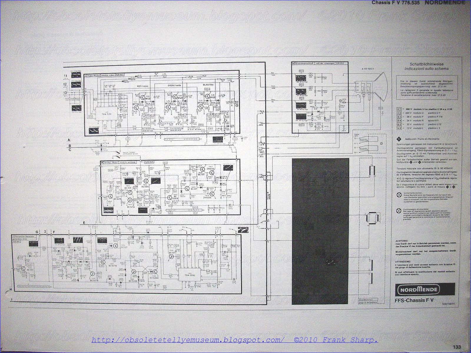
Horizontal deflection circuit
(Thyristor Horizontalsteuerung)


Description:
1. A horizontal deflection circuit for generating the deflection current in the deflection coil of a television picture tube wher
 ein a first switch controls the horizontal sweep, and wherein a second switch in a so-called commutation circuit with a commutating inductor and a commutating capacitor opens the first switch and, in addition, controls the energy transfer from a dc voltage source to an input inductor, characterized in that the input inductor (Le) and the commutating inductor (Lk) are combined in a unit designed as a transformer (U) which is proportioned so that the open-circuit inductance of the transformer is essentially equal to the value of the input inductor (Le), while the short-circuit inductance of the transformer (U) is essentially equal to the value of the commutating inductor (Lk), and that the second switch (S2) is connected in series with the dc voltage source (UB) and a first winding (U1) of the transformer (U). 2. A horizontal deflection circuit according to claim 1, characterized in that the transformer (U) operates as an isolation transformer between the supply (UB) and the subcircuits connected to a second winding. 3. A horizontal deflection circuit according to claim 1, characterized in that the second switch (S2) is connected between ground and that terminal of the first winding (U1) of the transformer (U) not connected to the supply potential (+UB). 4. A horizontal deflection circuit according to claim 1, characterized in that a capacitor (CE) is connected across the series combination of the first winding (U1) of the transformer and the second switch (S2). 5. A horizontal deflection circuit according to claim 1, characterized in that the second winding (U2) of the transformer (U) is connected in series with a first switch (S1), the commutating capacitor (Ck), and a third, bipolar switch (S3) controllable as a function of the value of a controlled variable developed in the deflection circuit. 6. A horizontal deflection circuit according to claim 5, characterized in that the third switch (S3) is connected between ground and the second winding (U2) of the transformer. 7. A horizontal deflection circuit according to claim 2, characterized in that the isolation transformer carries a third winding via which power is supplied to the audio output stage of the television set. 8. A horizontal deflection circuit according to claims 2, characterized in that the voltage serving to control the first switch (S1) is derived from a third winding of the transformer.
 German Aus
The first controlled switch also forms part of a second branch circuit where it is connected in series with a second current source and a reactance capable of oscillating. When the first switch is closed, the reactance, consisting essentially of a coil and a capacitor, receives energy from the second current source during a fixed time interval. This energy which is taken from the second current source corresponds to the circuit losses caused during the previous deflection cycle.
As can be seen, such a circuit needs two different, separate inductive elements, it being known that inductive elements are expensive to manufacture and always have a certain volume determined by the electrical properties required.
The object of the invention is to reduce the amount of inductive elements required.
The invention is characterized in that the input inductor and the commutating inductor are combined in a unit designed as a transformer which is proportioned so that the open-circuit inductance of the transformer is essentially equal to the value of the input inductor, while the short-circuit inductance of the transformer is essentially equal to the value of the commutating inductor, and that the second switch is connected in series with the dc voltage source and a first winding of the transformer.
This solution has an added advantage in that, in mass production, both the open-circuit and the short-circuit inductance are reproducible with reliability.
According to another feature of the invention, the electrical isolation between the windings of the transformer is such that the transformer operates as an isolation transformer between the supply and the subcircuits connected to a second winding or to additional windings of the transformer. In this manner, the transformer additionally provides reliable mains isolation.
According to a further feature of the invention, the second switch is connected between ground and that terminal of the first winding of the transformer not connected to the supply potential. This simplifies the control of the switch.
According to a further feature of the invention, to regulate the energy supply, the second winding of the transf
 ormer is connected in series with the first switch, the commutating capacitor, and a third, bipolar switch controllable as a function of the value of a controlled variable developed in the deflection circuit.
The advantage gained by this measure lies in the fact that the control takes place on the side separated from the mains, so no separate isolation device is required for the gating of the third switch. Further details and advantages will be apparent from the following description of the accompanying drawings and from the claims. In the drawings,
FIG. 1 is a basic circuit diagram of the arrangement disclosed in German Auslegeschrift (DT-AS) No. 1,537,308;
FIG. 2 shows a first embodiment of the horizontal deflection circuit according to the invention, and
FIG. 3 shows a development of the horizontal deflection circuit according to the invention.
FIG. 1 shows the essential circuit elements of the horizontal deflection circuit known from the German Auslegeschrift (DT-AS) No. 1,537,308 referred to by way of introduction.
Connected in series with a dc voltage source UB is an input inductor Le and a bipolar, controlled switch S2. In the following, this switch will be referred to as the "second switch"; it is usually called the "commutating switch" to indicate its function.
In known circuits, the second switch S2 consists of a controlled rectifier and a diode connected in inverse parallel.
The second switch S
2 also forms part of a second circuit which contains, in addition, a commutating inductor Lk, a commutating capacitor Ck, and a first switch S1. The first switch S1, controlling the horizontal sweep, is constructed in the same manner as the above-described second switch S2, consisting of a controlled rectifier and a diode in inverse parallel. Connected in parallel with this first switch is a deflection-coil arrangement AS with a capacitor CA as well as a high voltage generating arrangement (not shown). In FIGS. 1, 2, and 3, this arrangement is only indicated by an arrow and by the reference characters Hsp. The operation of this known horizontal deflection circuit need not be explained here in detail since it is described not only in the German Auslegeschrift referred to by way of introduction, but also in many other publications. FIGS. 2 and 3 show the horizontal deflection circuit modified in accordance with the present invention. Like circuit elements are designated by the same reference characters as in FIG. 1.
FIG. 2 shows the basic principle of the invention. The two inductors Le and Lk of FIG. 1 have been replaced by a transformer U. To be able to serve as a substitute for the two inductors Le and Lk, the transformer must be proportioned in a special manner. Regardless of the turns ratio, the open-circuit inductance of the transformer is chosen to be essentially equal to the value of the input inductor Le, and the short-circuit inductance of the transformer is essentially equal to the value of the commutating inductor Lk.
To permit the second switch S2 to be utilized for the connection of the dc voltage source UB, it is included in the circuit of that winding U1 of the transformer connected to the dc voltage UB.
In principle, it is of no consequence for the operation of the switch S2 whether it is inserted on that side of the winding U1 connected to the positive operating potential +UB or on the side connected to ground. In practice, however, the solution shown in FIGS. 2 and 3 will be chosen since the gating of the controlled rectifier is less problematic in this case.
In compliance with pertinent safety regulations, the transformer U may be designed as an isolation transformer and can thus provide mains separation, which is necessary for various reasons. It is known from German Offenlegungschrift (DT-OS) No. 2,233,249 to provide dc isolation by designing the commutating inductor as a transformer, but this measure is not suited to attaining the object of the present invention.
If the energy to be taken from the dc voltage source is to be controlled as a function of the energy needed in the horizontal deflection circuit and in following subcircuits, the embodiment of the horizontal deflection circuit of FIG. 3 may be used.
The circuit including the winding U2 of the transformer U contains a third controlled switch S3, which, too, is inserted on the grounded side of the winding U2 for the reasons mentioned above. This third switch S3, just as the second switch S2, is operated at the frequency of a horizontal oscillator HO, but a control circuit RS whose input l is fed with a controlled variable is inserted between the oscillator and the switch S3. Depending on this controlled variable, the controlled rectifier of the third switch S3 can be caused to turn on earlier. A suitable controlled variable containing information on the energy consumption is, for example, the flyback pulse capable of being taken from the high voltage generating circuit (not shown). Details of the operation of this kind of energy control are described in applicant's German Offenlegungsschrift (DT-OS) No. b 2,253,386 and do not form part of the present invention.
With mains isolation, the additional, third switch S3 shown here has the advantage of being on the side isolated from the mains and eliminates the need for an isolation device in the control lead of the controlled rectifier.
As an isolation transformer, the transformer U may also carry additional windings U3 and U4 if power is to be supplied to the audio output stage, for example; in addition, the first switch S1 may be gated via such an additional winding.
The points marked at the windings U1 and U2 indicate the phase relationship between the respective voltages. Connected in parallel with the winding U1 and the second switch S2 is a capacitor CE which completes the circuit for the horizontal-frequency alternating current; this serves in particular to bypass the dc voltage source or the electrolytic capacitors contained therein.
If required, a well-known tuning coil may be inserted, e.g. in series with the second winding U2, without changing the basic operation of the horizontal deflection circuit according to the invention.
NORDMENDE CHASSIS F5 Electron beam deflection circuit including thyristors Further Discussion and deepening of knowledge, Thyristor horizontal output circuits: (ZEILEN ABLENKUNG MIT THYRISTOR SCHALTUNG)
1. An electron beam deflection circuit for a cathode ray tube with electromagnetic deflection by means of a sawtooth current waveform having a trace portion and a retrace portion, said circuit comprising: a deflection winding; a first source of electrical energy formed by a first capacitor; first controllable switching means comprising a parallel combination of a first thyristor and a first diode connected together to conduct in opposite directions, for connecting said winding to said first source during said trace portion, while said first switching means is turned on; a second source of electrical energy including a first inductive energy storage means coupled to a voltage supply; reactive circuit means including a combination of inductive and capacitive reactances for storing the energy supplied by said second source; second controllable switching means, substantially similar to said first one, for completing a circuit including said reactive circuit means and said first switching means, when turned on before the end of said trace portion, so as to pass through said first switching means an oscillatory current in opposite direction to that which passes through said first thyristor from said first source and to turn said first thyristor off after these two currents cancel out, the oscillatory current flowing thereafter through said first diode for an interval termed the circuit turn-off time, which has to be greater than the turn-off time of said first thyristor; wherein the improvement comprises: means for drawing, during at least a part of said trace portion, a substantial amount of additional current through said first switching means, in the direction of conduction of said first diode, whereby to perceptibly shift the waveform of the current flowing through said first switching means towards the negative values by an amount equal to that of said substantial additional current and to lengthen, in proportion thereto, said circuit turn-off time, without altering the values of the reactances in the reactive circuit which intervene in the determination of both the circuit turn-off and retrace portion time intervals.
2. A deflection circuit as claimed in claim 1, wherein said amount of additional current is greater than or equal to 5 per cent of the peak-to-peak value of the current flowing through the deflection winding.
3. A deflection circuit as claimed in claim 1, wherein said means for drawing a substantial amount of additional current through said first switching means comprises a resistor connected in parallel to said first capacitor.
4. A deflection circuit as claimed in claim 1, wherein said means for drawing an additional current is formed by connecting said first and second energy sources in series so that the current charging said reactive circuit means forms the said additional current.
5. A deflection circuit as claimed in claim 1, further including a series combination of an autotransformer winding and a second high-value capacitor, said combination being connected in parallel to said first switching means, wherein said autotransformer comprises an intermediate tap located between its terminals respectively connected to said first switching means and to said second capacitor, said tap delivering, during said trace portion, a suitable DC supply voltage lower than the voltage across said second capacitor; and wherein said means for drawing a substantial amount of additional current comprises a load to be fed by said supply voltage and having one terminal connected to ground; and further controllable switching means controlled to conduct during at least part of said trace portion and to remain cut off during said retrace portion, said further switching means being connected between said tap and the other terminal of said load.
Description:
The present invention relates to electron beam deflection circuits including thyristors, such as silicon controlled rectifiers and relates, in particular, to horizontal deflection circuits for television receivers. The present invention constitutes an improvement in the circuit described in U.S. Pat. No. 3,449,623 filed on Sept. 6, 1966, this circuit being described in greater detail below with reference to FIGS. 1 and 2 of the accompanying drawings. A deflection circuit of this type comprises a first thyristor switch which allows the conenction of the horizontal deflection winding to a constant voltage source during the time interval used for the transmisstion of the picture signal and for applying this signal to the grid of the cathode ray tube (this interval will be termed the "trace portion" of the scan), and a second thyristor switch which provides the forced commutation of the first one by applying to it a reverse current of equal amplitude to that which passes through it from the said voltage source and thus to initiate the retrace during the horizontal blanking interval.
A undirectional reverse blocking triode type thyristor or silicon controlled rectifier (SCR), such as that used in the aformentioned circuit, requires a certain turn-off time between the instant at which the anode current ceases and the instant at which a positive bias may be applied to it without turning it on, due to the fact that there is still a high concentration of free carriers in the vicinity of the middle junction, this concentration being reduced by a process of recombination independently from the reverse polarity applied to the thyristor. This turn-off time of the thyristor is a function of a number of parameters such as the junction temperature, the DC current level, the decay time of the direct current, the peak level of the reverse current applied, the amplitude of the reverse anode to cathode voltage, the external impedance of the gate electrode, and so on, certain of these varying considerably from one thyristor to another.
In horizontal deflection circuits for television receivers, the flyback or retrace time is limited to approximately 20 percent of the horizontal scan period, the retrace time being in the case of the CCIR standard of 625 lines, approximately 12 microseconds and, in the case of the French standard of 819 lines, approximately 9 microseconds. During this relatively short interval, the thyristor has to be rendered non-conducting and the electron beam has to be returned to the origin of the scan. The first thyristor is blocked by means of a series resonant LC circuit which is subject to a certain number of restrictions (limitations as to the component values employed) due to the fact that, inter alia, it simultaneously determines the turn-off time of the circuit which blocks the thyristor and it forms part of the series resonant circuit which is to carry out the retrace. To obtain proper operation of the deflection circuit of the aforementioned Patent, especially when used for the French standard of 819 lines per image, the values of the components used have to subject to very close tolerances (approximately 2%), which results in high costs.
The improved deflection circuit, object o
f the present invention, allows the lengthening of the turn-off time of the circuit for turning the scan thyristor off, without altering the values of the LC circuit, which are determined by other criteria, and without impairing the operation of the circuit.According to the invention, there is provided an electron beam deflection circuit for a cathode ray tube with electromagentic deflection by means of a sawtooth current waveform having a trace portion and a retrace portion, said circuit comprising: a deflection winding; a first source of electrical energy formed by a first capacitor; first controllable switching means comprising a parallel combination of a first thyristor and a first diode, connected together to conduct in opposite directions, for connecting said winding to said first source during said trace portion when said first switching means is turned on; a second source of electrical energy including a first inductive energy storage means coupled to a voltage supply; reactive circuit means including a combination of inductive and capacitive reactances for storing the energy supplied by the said second source; a second controllable switching means, substantially identical with the first one, for completing a circuit including said reactive circuit means and said first switching means, when turned on, so as to pass through said first thyristor an oscillatory current in the opposite direction to that which passes through it from said first source and to turn it off after these two currents cancel out, the oscillatory current then flowing through said first diode for an interval termed the circuit turn-off time which has to be greater than the turn-off time of said first thyristor; and means for drawing duing at least a part of said trace portion a substantial amount of additional current from said first switching means in the direction of conduction of said first diode, whereby said circuit turn-off time is lengthened in proportion to the amount of said additional current, without altering the values of the reactances in the reactive circuit by shifting the waveform of the current flowing through said first switching means towards the negative by an amount equal to that of said additional current.
A further object of the invention consists in using the supplementary current in the recovery diode of the first switching means to produce a DC voltage which may be used as a power supply for the vertical deflection circuit of the television receiver, for example.
The invention will be better understood and other features and advantages thereof will become apparent from the following description and the accompanying drawings, given by way of example, and in which:
FIG. 1 is a schematic circuit diagram partially in bloc diagram form of a prior art deflection circuit according to the aforementioned Patent;
FIG. 2 shows waveforms of currents and voltages generated at various points in the circuit of FIG. 1;FIG. 3 is a schematic diagram of a deflection circuit according to the invention which allows the principle of the improvement to be explained;
FIG. 4 is a diagram of the waveforms of the current through the first switching means 4, 5 of the circuit of FIG. 3;
FIG. 5 is a circuit diagram of another embodiment of the circuit according to the invention;
FIG. 6 is a schematic representation of the preferred embodiment of the circuit according to the invention; and
FIG. 7 shows voltage waveforms at various points of the high voltage autotransformer 21 of FIG. 6.
In all these Figures the same reference numerals refer to the same components.
FIG. 1 shows the horizontal deflection circuit described and claimed in the U.S. Pat. No. 3,449,623 mentioned above, which comprises a first source of electrical energy in the shape of a first capacitor 2 having a high capacitance C 2 for supplying a substantially constant voltage Uc 2 across its terminals. A first terminal of the first capacitor 2 is connected to ground, whilst its second terminal which supplies a positive voltage is connected to one of the terminals of a horizontal deflection winding shown as a first inductance 1. A first switching means 3, consisting of a first reverse blocking triode thyristor 4 (SCR) and a first recovery diode 5 in parallel, the two being interconnected to conduct current in opposite directions, is connected in parallel with the series combination formed by the deflection winding 1 and the first capacitor 2. The assembly of components 1, 2, 4 and 5 forms the final stage of the horizontal deflection circuit in a television receiver using electromagnetic delfection.The deflection circuit also includes a drive stage for this final stage which here controls the turning off of the first thyristor 4 to produce the retrace or fly-back portion of the scan during the line-blanking intervals i.e. while the picture signal is not transmitted. This driver stage comprises a second voltage source in the shape of a DC power supply 6 which delivers a constant high voltage E. The negative terminal of the power supply 6 is connected to ground and its positive terminal to one of the terminals of a second inductance 7 of relatively high value, which draws a substantially lineraly varying current from the power supply 6 to avoid its overloading. The other terminal of th
e second inductance 7 is connected, on the one hand, to the junction of the deflection winding 1 and the first switching means 3 by means of a second inductance 8 and a second capacitor 9 in series and, on the other hand, to one of the terminals of a second controllable bi-directionally conducting switching means 10, similar to the first one 3, including a parallel combination of a second thyristor 11 and a second recovery diode 12 also arranged to conduct in opposite directions.The respective values of the third inductance 8 (L 8 ) and of the second capacitor 9 (C 9 ) are principally selected so that, on the one hand, one half-cycle of oscillation of the first series resonant circuit L 8 - C 9 , (i.e. π √ L 8 . C 9 ) is longer than the turn-off time of the first thyristor 4, but still is as short as possible since this time interval determines the speed of the commutation of the thyristor 4, and, on the other hand, one half-cycle of oscillation of another series resonant circuit formed by L 1 , L 8 and C 9 , i.e. π √ (L 1 + L 8 ) . C 9 , is substantially equal to the required retrace time interval (i.e. shorter than the horizontal blanking interval).
The gate (control electrode) of the second thyristor 11 is coupled to the output of the horizontal oscillator 13 of the television receiver by means of a first pulse transformer 14 and a first pulse shaping circuit 15 so that it is fed short triggering pulses which are to turn it on.
The gate of the first thyristor 4 fed with signals of a substantially rectangular waveform which are negative during the horizontal blanking intervals, is coupled to a winding 16 by means of a second pulse shaping circuit 17, the winding 16 being magnetically coupled to the second inductance 7 to make up the secondary winding of a transformer of which the inductance 7 forms the primary winding. It will be noted here that it is also possible to couple the secondary winding 16 magnetically to a primary winding connected to a suitable output (not shown) of the horizontal oscillator 13.
The operation of a circuit of this type will be explained below with reference to FIG. 2 which shows the waveforms at various points in the circuit of FIG. 1 during approximately one line period.
FIG. 2 is not to scale since one line period (t 7 - t 0 ) is equal to 64 microseconds in the case of 625 lines and 49 microseconds in the case of 819 lines, while the durations of the respective horizontal blanking intervals are approximately 12 and 9.5 microseconds.Waveform A shows the form of the current i L1 passing through deflection winding 1, this current having a sawtooth waveform substantially linear from t 0 to t 3 and from t 5 to t 7 , and crossing zero at time instants t 0 and t 7 , and reaching values of + I 1m and - I 1m , at time instants t 3 and t 5 respectively, these being its maximum positive and negative amplitudes.
During the second half of the trace portion of the horizontal deflection cycle, that is to say from t 0 to t 3 , the thyristor 4 of the first switching means 3 is conductive and makes the high value capacitor 2 discharge through the deflector winding 1, which has a high inductance, so that current i L1 increases linearly.
A few microseconds (5 to 8 μ s) before the end of the trace portion, i.e. at time instant t 1 , the trigger of the second thyristor 11 receives a short voltage pulse V G11 which causes it to turn on as its anode is at this instant at a positive potential with respect to ground, which is due to the charging of the second capacitor 9 through inductances 7 and 8 by the voltage E from the power supply 6.
When thyristor 11 is made conductive at time t 1 , on the one hand, inductance 7 is connected between ground and the voltage source 6 and a linearly increasing current flows through it and, on the other hand, the reactive circuit 8, 9 forms a loop through the second and first switching means 10 and 3, thus forming a resonant circuit which draws an oscillatory current i 8 ,9 of frequency ##EQU1##
This oscillatory current i 8 ,9 will pass through the first switching means 3, i.e. thyristor 4 and diode 5, in the opposite direction to that of current i L1 . Since the frequency f 1 is high, current i 8 ,9 will increase more rapidly than i L1 and will reach the same level at time t 2 , that is to say i 8 ,9 (t 2 ) = -i L1 (t 2 ) and these currents will cancel out in the thyristor 4 in accordance with the well known principle of forced commutation. After time instant t 2 , current i 8 ,9 continues to increase more rapidly than i L1 , but the difference between them (i 8 ,9 - i L1 ) passes the diode 5 (see wave form B) until it becomes zero at time instant t 3 which is the turn off time instant of the first switching means 3, at which the retrace begins.
The interval between the time instant t 2 and t 3 , i.e. (t 3 -t 2 ), during which diode 5 is conductive and the thyristor is reverse biased will be termed in what follows the circuit turn-off time and it should
be greater than the turn-off time of the thyristor 4 itself since the latter will subsequently become foward biased (i.e. from t 3 to t 5 ) by the retrace or flyback pulse (see waveform E) which should not trigger it.At time instant t 3 , the switching means 3 is opened (i 4 and i 5 are both zero -- see waveforms B and C) and the reactive circuit 8, 9 forms a loop through capacitor 2 and the deflection coil 1 and thus a series resonant circuit including (L 1 + L 8 ) and C 9 , C 2 being of high value and representing a short circuit for the flyback frequency ##EQU2## thus obtained.
The retrace which stated at time t 3 takes place during one half-cycle of the resonant circuit formed by reactances L 1 , L 8 and C 9 , i.e. during the interval between t 3 and t 5 . In the middle of this interval i.e. at time instant t 4 , both i L1 (waveform A) and i 8 ,9 (waveform D) pass through zero and change their sign, whereas the voltage at the terminals of the first switching means 3 (V 3 , waveform E) passes through a maximum. Thus, from t 4 onwards, thyristor 11 will be reverse biased and diode 12 will conduct the current from the resonant circuit 1, 8 and 9 in order to turn the second thyristor 11 off.
At time instant t 5 , when current i L1 has reached - I 1m and when voltage v 3 falls to zero, diode 5 of the first switching means 3 becomes conductive and the trace portion of scan begins.
Current i 8 ,9 nevertheless continues to flow in the resonant circuit 8, 9 through diodes 5 and 12, which causes a break to appear in waveform D at t 5 , and a negative peak to appear in waveform D and a positive one in waveform B in the interval between t 5 and t 6 , these being principally due to the distributed capacities of coil 1 or to an eventual capacitor (not shown) connected in parallel to the first switching means 3.
At time instant t 6 , diode 12 of the second switching means 10 ceases to conduct after having allowed thyristor 11 time to become turned off completely.
The level of current i 8 ,9 at time instant t 5 (i.e. I c ) as well as the negative peak I D12 in i 8 ,9 and the positive peak I D5 in i 5 depend on the values of L 8 and C 9 in the same way as does the turn-off time of the circuit (t 3 - t 2 ). If, for example, L 8 and C 9 , are increased I D5 increases towards zero and this could cause diode 5 to be cut off in an undesirable fashion. I c also increases towards zero, which is liable to cause diode 12 to be blocked and thyristor 11 to trigger prematurely.
From the foregoing it can be clearly seen that the choice of values for L 8 and C 9 is subject to four limitations which prevent the values from being increased to lengthen the turn-off time of the driver circuit of first switching thyristor 4 so as to forestall its spurious triggering.
Waveform F shows the voltage v G4 obtained at the gate of thyristor 4 from the secondary winding 16 coupled to the inductor 7. This voltage is positive from t 0 to t 1 and from t 6 to t 7 and is negative between t 2 and t 6 i.e. while the second switching means 10 is conducting.
The present invention makes the lengthening of the turn-off time of thyristor 4 possible without altering the parameters of the circuit such as inductance 8 and capacitor 9.
 In the circuit shown in FIG. 3, which illustrates the principle of the present invention, means are added to the circuit in FIG. 1 which enable the turn-off time to be lengthened by connecting a load to diode 5 so as to increase the current which flows through it during the time that it is conductive. These means are here formed by a resistor 18 connected in parallel with a capacitor 20 (which replaces capacitor 2) which is of a higher capacitance so that, in practice, it holds its charge during at least one half of the line period. FIG. 4, which shows the waveform of the current in the first switching means 3 for a circuit as shown in FIG. 3, makes it possible to explain how this lenthening of the turn-off time is achieved.
In FIG. 4, the broken lines show the waveform of the current in the first switch device 3 in the circuit of FIG. 1, this waveform being produced by adding waveforms B and C of FIG. 2. The current i 4 above the axis flows through thyristor 4 and current i 5 below the axis flows through diode 5. When the capacitance C 20 of the capacitor in series with the deflector coil is increased to some tens of microfarads (C 2 having been of the order of 1 μ F) and when there is connected in parallel with capacitor 20 a resistor 18 the value of which is calculated to draw a strong current I R18 from capacitor 20, that is to say a current at least equal to 0,1 I m (I m being of the order of some tens of amperes), current I R18 is added to that i 5 which flows through diode 5 without in any way altering the linearity of the trace portion nor the oscillatory commutation of thyristor 4 which is brought about by the resonant circuit L 8 , C 9 .
The fact of loading capacitor C 20 by means of a resistor 18 thus has the effect of permanently displacing the waveform of the current in the negative direction by I R18 . Thus, during the trace portion of the scan, the transfer of the current from the diode 5 to the thyristor 4 begins at time t 10 instead of t 0 , that is to say with a delay proportional to I R18 . The effect of the triggering pulse delivered by the horizontal oscillator (13 FIG. 1) to the second thyristor 11 at time instant t 1 , will be to start the commutation process of the first thyristor 4 when the current it draws is less by I R18 than that i 4 (t 1 ) which it would have been drawing had there been no resistor 18. Because of this, the turn-off time of the thyristor 4 proper, which as has been mentioned increases with the maximum current level passing throught it, is slightly reduced. Moreover, because the oscillatory current i 8 ,9 (FIG. 2) from circuit L 8 , C 9 which flows through thyristor 4 in the opposite direction is unchanged, it reaches a value equal to that of the current i L1 (FIG. 1) flowing in the coil 1 in a shorter time, that is to say at time t 12 . Diode 5 will thus take the oscillatory current i 8 ,9 (FIG. 2) over in advance with respect ro time instant t 2 and will conduct it until it reaches zero value at a time instant t 13 later than t 3 , the amounts of advance (t 2 - t 12 ) and delay (t 13 - t 3 ) being practically equal.
It can thus be seen in FIG. 4 that the circuit turn-off time T R of a circuit according to the invention and illustrated by FIG. 3 is distinctly longer than that T r of the circuit in FIG. 1. This increase in the turn-off time (T R - T r ) depends on the current I R18 and increases therewith.It should be noted at this point that the current I R18 produces a voltage drop at the terminals of the resistor the only effect of which is to heat up the resistor since the level of this voltage (40 to 60 volts) does not necessarily have a suitable value to be used as a voltage supply for other circuits in an existing transistorised television receiver.
In accordance with one embodiment of the invention, illustrated in FIG. 5, an application is proposed for the additional current which is to be drawn through diode 5. In FIG. 5, the positive terminal of capacitor 20 is connected by a conductor 19 to the negative pole of the power supply 6 and the voltage at the terminals of capacitor 20 is thus added to that E from the source 6.
In the preferred embodiment of the present invention, which is shown in FIG. 6, it is possible to cause a supplementary current of a desired value to flow through the first diode 5 while obtaining a voltage which has a suitable value for use in another circuit in the television receiver.
If the voltage at the terminals of capacitor 20 in FIG. 3 is not a usable value, it is possible to connect in parallel with the series circuit comprising the deflector coil 1 and the capacitor 2 in FIG. 1, i.e. in parallel with the terminals of the first switching means 3, a series combination of an autotransformer 21 and a high value capacitor 22 (comparable with capacitor 20 in FIGS. 3 and 5). The autotransformer 21 has a tap 23 is suitably positioned between the terminal connected to capacitor 22 at the tap 24 connected to the first switching means 3. This autotransformer 21 may be formed by the one conventionally used for supplying a very high voltage to the cathode ray tube, as described for example in U.S. Pat. No. 3,452,244; such a transformer comprises a voltage step-up winding between taps 24 and 25, which latter is connected to a high voltage rectifier (not shown).
The voltage V c22 at the terminals of capacitor 22 varies slightly about a mean value V cm . It is increasing while diode 5 is conducting and decreasing during the conduction of the thyristor 4.
The voltage v 24 at tap 24 follows substantially the same curve as waveform E in FIG. 2, that is to say that during the retrace time interval from t 13 to t 5 to a positive pulse called the flyback pulse is produced and, during the time interval while the first switching means 3 is conducting, the voltage is zero. The mean valve of the voltage v 24 at tap 24 of the auto-transformer 21 is equal to the mean value V cm of the voltage at the terminals of capacitors 2 and 22.
Thus, there is obtained at tap 23 a waveform which is made up, during the retrace portion, of a positive pulse whose maximum amplitude is less than that of v 24 at tap 24 and, during the trace portion, of a substantially constant positive voltage, the level V of which is less than the mean value V cm of the voltage v c22 at the terminals of capacitor 22. By moving tap 23 towards terminals 24 the amplitude of the pulse during fly-back increases while voltage V falls and conversely by moving tap 23 towards capacitor 22 voltage V increases and the amplitude of the pulse drops.
In more exact terms, the voltage V at tap 23 is such that the means value of v 23 is equal to V cm . It has thus been shown that by choosing carefully the position of tape 23, a voltage V may be obtained during the trace portion of the scan, which may be of any value between V cm and zero.
It may easily be seen that the DC collector/emitter current in transistor 26 flows through the first diode 5 of the first switching means 3 via a resistor 28 and the part of the winding of auto-transformer 21 located between taps 23 and 24.
Experience has shown that a circuit as shown in FIG. 6 can supply 24 volts with a current of 2 amperes to the vertical deflection circuit of the same television set, the voltage at the terminals of capacitor 22 being from 50 to 60 volts.
It should be mentioned that, when the circuit which forms the load of the controlled rectifier 26, 27 does not draw enough current to sufficiently lengthen the circuit turn-off time T R , an additional resistor (not shown) may be connected between the emitter of transistor 26 and ground or in parallel to capacitor 22, which resistor will draw the additional current required.
NORDMENDE SPECTRA SK2-COLOR DE LUXE CONTURA CHASSIS F5 Gating circuit for television SCR deflection system AND REGULATION / stabilization of horizontal deflection NETWORK CIRCUIT with Transductor reactor / Reverse thyristor energy recovery circuit.
In a television deflection system
employing a first SCR for coupling a deflection winding across a source of energy during a trace interval of each deflection cycle and a second SCR for replenishing energy to the source of energy during a commutation interval of each deflection cycle, a gating circuit for triggering the first SCR. The gating circuit employs a voltage divider coupled in parallel with the second SCR which develops gating signals proportional to the voltage across the second SCR.
1. In a television deflection system in which a first switching means couples a deflection winding across a source of energy during a trace interval of each deflection cycle and a second switching means replenishes energy to said source of energy during a commutation interval of each deflection cycle, a gating circuit for said first switching means, comprising:
capacitive voltage divider means coupled in parallel with said second switching means for developing gating signals proportional to the voltage across said second switching means; and
means for coupling said voltage divider means to said first switching means to provide for conduction of said first switching means in response to said gating signals.
2. A gating circuit according to claim 1 wherein said voltage divider includes first and second capacitors coupled in series and providing said gating signals at the common terminal of said capacitors. 3. A gating circuit according to claim 2 wherein said first and second capacitors are proportional in value to provide for the desired magnitude of gating signals. 4. A gating circuit according to claim 3 wherein said means for coupling said voltage divider means to said first switching means includes an inductor. 5. A gating circuit according to claim 4 wherein said inductor and said first and second capacitors comprise a resonant circuit having a resonant frequency chosen to shape said gating signal to improve switching of said first switching means.
Description:
BACKGROUND OF THE INVENTION
 This invention relates to a gating circuit for controlling a switching device employed in a deflection circuit of a television receiver.


Various deflection system designs have been utilized in television receivers. One design employing two bidirectional conducting switches and utilizing SCR's (thyristors) as part of the switches is disclosed in U.S. Pat. No. 3,452,244. In this type deflection system, a first SCR is


 employed for coupling a deflection winding across a source of energy during a trace interval of each deflection cycle, and a second SCR is employed for replenishing energy during a commutation interval of each deflection cycle. The first SCR is commonly provided with gating voltage by means of a separate winding or tap of an input reactor coupling a source of B+ to the second SCR.
Various regulator system designs have been utilized in conjunction with the afore described deflection system to provide for uniform high voltage production as well as uniform picture width with varying line voltage and kinescope beam current conditions.
One type regulator system design alters the amount of energy stored in a commutating capacitor coupled between the first and second SCR's during the commutating interval. A regulator design of this type may employ a regulating SCR and diode for coupling the input reactor to the source of B+. With this type regulator a notch, the width of which depends upon the regulation requirements, is created in the current supplied through the reactor and which notch shows up in the voltage waveform developed on the separate winding or tap of the input reactor which provides the gating voltage for the first SCR. The presence of the notch, even though de-emphasized by a waveshaping circuit coupling the gating voltage to the first SCR, causes erratic control of the first SCR.
SUMMARY OF THE INVENTION
In accordance with one embodiment of the invention, a gating circuit of a television deflection system employing a first switching means for coupling a deflection winding across a source of energy during a trace interval of each deflection cycle and a second switching means for replenishing energy to said source of energy during a commutation interval of each deflection cycle includes a voltage divider means coupled in parallel with the second switching means for developing gating signals proportional to the voltage across the second switching means. The voltage divider means are coupled to the first switching means to provide for conduction of the first switching means in response to the gating signals.
A more detailed description of a preferred embodiment of the invention is given in the following description and accompanying drawing of which:
FIG. 1 is a schematic diagram, partially in block form, of a prior art SCR deflection system;
FIG. 2 is a schematic diagram, partially in block form, of an SCR deflection system of the type shown in FIG. 1 including a gating circuit embodying the invention;
FIG. 3 is a schematic diagram, partially in block form, of one type of a regulator system which employs an SCR as a control device and which is suitable for use with the SCR deflection system of FIG.2;
FIG. 4 is a schematic diagram, partially in block form, of another type of a regulator system suitable for use with the deflection circuit of FIG. 2; and
FIG. 5 is a schematic diagram, partially in block form, of still another type of a regulator system suitable for use with the SCR deflection system of FIG. 2.
DESCRIPTION OF THE PREFERRED EMBODIMENT
FIG. 1 is a schematic diagram, partially in block form, of a prior art deflection system of the retrace driven type similar to that disclosed in U.S. Pat. No. 3,452,244. This system includes a commutating switch 12, comprising a silicon controlled rectifier (SCR) 14 and an oppositely poled damper diode 16. The commutating switch 12 is coupled between a winding 18a of an input choke 18 and ground. The other terminal of winding 18a is coupled to a source of direct current voltage (B+) by means of a regulator network 20 which controls the energy stored in the deflection circuit 10 when the commutating switch is off, during an interval T3 to T0' as shown in curve 21 which is a plot of the voltage level at the anode of SCR 14 during the deflection cycle. A damping network comprising a series combination of a resistor 22 and a capacitor 23 is coupled in parallel with commutating switch 12 and serves to reduce any ringing effects produced by the switching of commutating switch 12. Commutating switch 12 is coupled through a commutating coil 24, a commutating capacitor 25 and a trace switch 26 to ground. Trace switch 26 comprises an SCR 28 and an oppositely poled damper diode 30. An auxiliary capacitor 32 is coupled between the junction of coil 24 and capacitor 25 and ground. A series combination of a horizontal deflection winding 34 and an S-shaping capacitor 36 are coupled in parallel with trace switch 26. Also, a series combination of a primary winding 38a of a horizontal output transformer 38 and a DC blocking capacitor 40 are coupled in parallel with trace switch 26.
A secondary of high voltage winding 38b of transformer 38 produces relatively large amplitude flyback pulses during the retrace interval of each deflection cycle. This interval exists between T1 and T2 of curve 41 which is a plot of the current through windings 34 and 38a during the deflection cycle. These flyback pulses are applied to a high voltage multiplier (not shown) or other suitable means for producing direct current high voltage for use as the ultor voltage of a kinescope (not shown).
An auxiliary winding 38c of transformer 38 is coupled to a high voltage sensing and control circuit 42 which transforms the level of flyback pulses into a pulse width modulated signal. The control circuit 42 is coupled to the regulator network 20.
A horizontal oscillator 44 is coupled to the gate electrode of commutating SCR 14 and produces a pulse during each deflection cycle slightly before the end of the trace interval at T0 of curve 21 to turn on SCR 14 to initiate the commutating interval. The commutating interval occurs between T0 and T3 of curve 21. A resonant waveshaping network 46 comprising a series combination of a capacitor 48 and an inductor 50 coupled between a winding 18b of input choke 18 and the gate electrode of trace SCR 28 and a damping resistor 52 coupled between the junction of capacitor 48 and inductor 50 and ground shapes the signal developed at winding 18b (i.e. voltage waveform 53) to form a gating signal voltage waveform 55 to enable SCR 28 for conduction during the second half of the trace interval occurring between T2 and T1' of curve 41.
 The regulator network 20, when of a type to be described in conjunction with FIG. 3, operates in such a manner that current through winding 18a of input choke 18 during an interval between T4 and T5 (region A) of curves 21, 53 and 55 is interrupted for a period of time the duration of which is determined by the signal produced by the high voltage sensing and control circuit 42. During the interruption of current through winding 18a a zero voltage level is developed by winding 18b as shown in interval T4 to T5 of curve 53. The resonant waveshaping circuit 46 produces the shaped waveform 55 which undesirably retains a slump in region A corresponding to the notch A of waveform 53. The slump in waveform 55 applied to SCR 28 occurs in a region where the anode of SCR 28 becomes positive and where SCR 28 must be switched on to maintain a uniform production of the current waveshape in the horizontal deflection winding 34 as shown in curve 41. The less positive amplitude current occurring at region A of waveform 55 may result in insufficient gating current for SCR 28 and may cause erratic performance resulting in an unsatisfactory raster.
FIG. 2 is a schematic diagram, partially in block form, of a deflection system 60 embodying the invention. Those elements which perform the same function in FIG. 2 as in FIG. 1 are labeled with the same reference numerals. FIG. 2 differs from FIG. 1 essentially in that the signal to enable SCR 28 derived from sampling a portion of the voltage across commutating switch 12 rather than a voltage developed by winding 18b which is a function of the voltage across winding 18a of input choke 18 as in FIG. 1. This change eliminates the slump in the enabling signal during the interval T4 to T5 as shown in curve 64 since the voltage across the commutating switch 12 is not adversely effected by the regulator network 20 operation.
A series combination of resistor 22, capacitor 23 and a capacitor 62 is coupled in parallel with commutating switch 12, one terminal of capacitor 62 being coupled to ground. The junction of capacitors 23 and 62 is coupled to the gate electrode of SCR 28 by means of the inductor 50. The resistor 52 is coupled in parallel with capacitor 62.
Capacitors 23 and 62 form a capacitance voltage divider which provides a suitable portion of the voltage across commutating switch 12 for gating SCR 28 via inductor 50. The magnitude of the voltage at the junction of capacitors 23 and 62 is typically 25 to 35 volts. It can, therefore, be seen that the ratio of values of capacitors 23 and 62 will vary depending on the B+ voltage utilized to energize the deflection system. Capacitors 23 and 62 and inductor 50 form a resonant circuit tuned in a manner which provides for peaking of the curve 64 between T4 and T5. This peaking effect further enhances gating of SCR 28 between T4 and T5.
Since the waveshape of the voltage across commutating switch 12 (curve 21) is relatively independent of the type of regulator system employed in conjunction with the deflection system, the curve 64 also is independent of the type of regulator system.
When commutating switch 12 switches off during the interval T3 to T0' curve 21, the voltage across capacitor 62 increases and the voltage at the gate electrode of SCR 28 increases as shown in curve 64. As will be noted, no slump of curve 64 occurs between T3 and T5 because there is no interruption of the voltage across commutating switch 12.


FIG. 3 is a schematic diagram, partially in block form, of one type of a regulator system which may be used in conjunction with the invention. B+ is supplied through a regulator network 20 which comprises an SCR 66 and an oppositely poled diode 68. The diode is poled to provide for conduction of current from B+ to the horizontal deflection circuit 60 via winding 18a of input choke 18. Current flows through the diode during the period T3 to T4 of curve 21 FIG. 1 after which current tries to flow through the SCR 66 from the horizontal deflection circuit to B+ since the commutating capacitor 25 is charged to a voltage higher than B+.
The horizontal deflection circuit 60 produces a flyback pulse in winding 38a of the flyback transformer 38 which is coupled to winding 38c. The magnitude of the pulse on winding 38c determines how long the signal required to switch SCR 66 on is delayed after T4 curve 21 FIG. 1. If the flyback pulse is greater than desirable, the SCR 66 turns on sooner than if the flyback pulse is less than desirable and provides a discharge path for current in commutating capacitor 25 back to the B+ supply. In this manner a relatively constant amplitude flyback pulse is maintained.
FIG. 4 is a schematic diagram, partially in block form, of another well-known type of a regulator system which may be used in conjunction with the invention shown in FIG. 2. B+ is coupled through winding 18a of input choke 18 and through a series combination of windings 70a and 70b of a saturable reactor 70 and a parallel combination of a diode 72 and a resistor 74 to the horizontal deflection circuit 60. Diode 72 is poled to conduct current from the horizontal deflection circuit 60 to B+.
Flyback pulse variations are obtained from winding 38c of the horizontal output transformer 38 and applied to a voltage divider comprising resistors 76, 78 and 80 of the high voltage sensing and control circuit 42. A portion of the pulse produced by winding 38c is selected by the position of the wiper terminal on potentiometer 78 and coupled to the base electrode of a transistor 82 by means of a zener diode 84. The emitter electrode of transistor 82 is grounded and a DC stabilization resistor 85 is coupled in parallel with the base-emitter junction of transistor 82. When the pulse magnitude on winding 38c exceeds a level which results in forward biasing the base-emitter junction of transistor 82, current flows from B+ through a resistor 86, a winding 70c of saturable reactor 70 and transistor 82 to ground. Due to the exponential increase of current in winding 70c during the period of conduction of transistor 82, the duration of conduction of transistor 82 determines the magnitude of current flowing in winding 70c and thus the total inductance of windings 70a and 70b. The current in winding 70c is sustained during the remaining deflection period by means of a diode 88 coupled in parallel with winding 70c and poled not to conduct current from B+ to the collector electrode of transistor 82. A capacitor 90 coupled to the cathode of diode 88 provides a bypass for B+. Windings 70a and 70b are in parallel with input reactor 18a and thereby affect the total input inductance of the deflection circuit and thereby controls the transfer of energy to the deflection circuit. The dotted waveforms shown in conjunction with a curve 21' indicate variations from a nominal waveform provided at the input of horizontal deflection circuit 60 by the windings 70a and 70b.


FIG. 5 is a schematic diagram of yet another type of a regulator system which may be used in conjunction with the invention. B+ is coupled through a winding 92a and a winding 92b of a saturable reactor to the horizontal deflection circuit 60. Windings 92a and 92b are used to replace the input choke 18 shown in FIGS. 1 and 2 while also providing for a regulating function corresponding to that provided by regulating network 20.
Flyback pulse variations are obtained from winding 38c and applied to the high voltage sensing and control circuit 42 as in FIG. 4. Current flows from B+ through resistor 86, a winding 92c and transistor 82 to ground. As in FIG. 4 the duration of the conduction of transistor 82 determines the energy stored in winding 92c and thus the total inductance of windings 92a and 92b which control the amount of energy transferred to the deflection circuit during each horizontal deflection cycle. The variations in waveforms of curve 21', shown in conjunction with FIG. 4, are also provided at the input of horizontal deflection circuit 60 by windings 92a and 92b.
For various reasons including cost or performance, a manufacturer may wish to utilize a particular one of the regulators illustrated in FIGS. 3, 4 and 5. Regardless of the choice, the gating circuit according to the invention may be utilized therewith advantageously by providing improved performance and the possibility of cost savings by eliminating taps or extra windings on the wound components which heretofore normally provided a source of SCR gating waveforms.
This invention relates to a gating circuit for controlling a switching device employed in a deflection circuit of a television receiver. 


Various deflection system designs have been utilized in television receivers. One design employing two bidirectional conducting switches and utilizing SCR's (thyristors) as part of the switches is disclosed in U.S. Pat. No. 3,452,244. In this type deflection system, a first SCR is


Various regulator system designs have been utilized in conjunction with the afore described deflection system to provide for uniform high voltage production as well as uniform picture width with varying line voltage and kinescope beam current conditions.
One type regulator system design alters the amount of energy stored in a commutating capacitor coupled between the first and second SCR's during the commutating interval. A regulator design of this type may employ a regulating SCR and diode for coupling the input reactor to the source of B+. With this type regulator a notch, the width of which depends upon the regulation requirements, is created in the current supplied through the reactor and which notch shows up in the voltage waveform developed on the separate winding or tap of the input reactor which provides the gating voltage for the first SCR. The presence of the notch, even though de-emphasized by a waveshaping circuit coupling the gating voltage to the first SCR, causes erratic control of the first SCR.
SUMMARY OF THE INVENTION
In accordance with one embodiment of the invention, a gating circuit of a television deflection system employing a first switching means for coupling a deflection winding across a source of energy during a trace interval of each deflection cycle and a second switching means for replenishing energy to said source of energy during a commutation interval of each deflection cycle includes a voltage divider means coupled in parallel with the second switching means for developing gating signals proportional to the voltage across the second switching means. The voltage divider means are coupled to the first switching means to provide for conduction of the first switching means in response to the gating signals. A more detailed description of a preferred embodiment of the invention is given in the following description and accompanying drawing of which:
FIG. 1 is a schematic diagram, partially in block form, of a prior art SCR deflection system;
FIG. 2 is a schematic diagram, partially in block form, of an SCR deflection system of the type shown in FIG. 1 including a gating circuit embodying the invention;
FIG. 3 is a schematic diagram, partially in block form, of one type of a regulator system which employs an SCR as a control device and which is suitable for use with the SCR deflection system of FIG.2;
FIG. 4 is a schematic diagram, partially in block form, of another type of a regulator system suitable for use with the deflection circuit of FIG. 2; and
FIG. 5 is a schematic diagram, partially in block form, of still another type of a regulator system suitable for use with the SCR deflection system of FIG. 2.
DESCRIPTION OF THE PREFERRED EMBODIMENT
FIG. 1 is a schematic diagram, partially in block form, of a prior art deflection system of the retrace driven type similar to that disclosed in U.S. Pat. No. 3,452,244. This system includes a commutating switch 12, comprising a silicon controlled rectifier (SCR) 14 and an oppositely poled damper diode 16. The commutating switch 12 is coupled between a winding 18a of an input choke 18 and ground. The other terminal of winding 18a is coupled to a source of direct current voltage (B+) by means of a regulator network 20 which controls the energy stored in the deflection circuit 10 when the commutating switch is off, during an interval T3 to T0' as shown in curve 21 which is a plot of the voltage level at the anode of SCR 14 during the deflection cycle. A damping network comprising a series combination of a resistor 22 and a capacitor 23 is coupled in parallel with commutating switch 12 and serves to reduce any ringing effects produced by the switching of commutating switch 12. Commutating switch 12 is coupled through a commutating coil 24, a commutating capacitor 25 and a trace switch 26 to ground. Trace switch 26 comprises an SCR 28 and an oppositely poled damper diode 30. An auxiliary capacitor 32 is coupled between the junction of coil 24 and capacitor 25 and ground. A series combination of a horizontal deflection winding 34 and an S-shaping capacitor 36 are coupled in parallel with trace switch 26. Also, a series combination of a primary winding 38a of a horizontal output transformer 38 and a DC blocking capacitor 40 are coupled in parallel with trace switch 26. A secondary of high voltage winding 38b of transformer 38 produces relatively large amplitude flyback pulses during the retrace interval of each deflection cycle. This interval exists between T1 and T2 of curve 41 which is a plot of the current through windings 34 and 38a during the deflection cycle. These flyback pulses are applied to a high voltage multiplier (not shown) or other suitable means for producing direct current high voltage for use as the ultor voltage of a kinescope (not shown). An auxiliary winding 38c of transformer 38 is coupled to a high voltage sensing and control circuit 42 which transforms the level of flyback pulses into a pulse width modulated signal. The control circuit 42 is coupled to the regulator network 20.
A horizontal oscillator 44 is coupled to the gate electrode of commutating SCR 14 and produces a pulse during each deflection cycle slightly before the end of the trace interval at T0 of curve 21 to turn on SCR 14 to initiate the commutating interval. The commutating interval occurs between T0 and T3 of curve 21. A resonant waveshaping network 46 comprising a series combination of a capacitor 48 and an inductor 50 coupled between a winding 18b of input choke 18 and the gate electrode of trace SCR 28 and a damping resistor 52 coupled between the junction of capacitor 48 and inductor 50 and ground shapes the signal developed at winding 18b (i.e. voltage waveform 53) to form a gating signal voltage waveform 55 to enable SCR 28 for conduction during the second half of the trace interval occurring between T2 and T1' of curve 41.
 The regulator network 20, when of a type to be described in conjunction with FIG. 3, operates in such a manner that current through winding 18a of input choke 18 during an interval between T4 and T5 (region A) of curves 21, 53 and 55 is interrupted for a period of time the duration of which is determined by the signal produced by the high voltage sensing and control circuit 42. During the interruption of current through winding 18a a zero voltage level is developed by winding 18b as shown in interval T4 to T5 of curve 53. The resonant waveshaping circuit 46 produces the shaped waveform 55 which undesirably retains a slump in region A corresponding to the notch A of waveform 53. The slump in waveform 55 applied to SCR 28 occurs in a region where the anode of SCR 28 becomes positive and where SCR 28 must be switched on to maintain a uniform production of the current waveshape in the horizontal deflection winding 34 as shown in curve 41. The less positive amplitude current occurring at region A of waveform 55 may result in insufficient gating current for SCR 28 and may cause erratic performance resulting in an unsatisfactory raster. FIG. 2 is a schematic diagram, partially in block form, of a deflection system 60 embodying the invention. Those elements which perform the same function in FIG. 2 as in FIG. 1 are labeled with the same reference numerals. FIG. 2 differs from FIG. 1 essentially in that the signal to enable SCR 28 derived from sampling a portion of the voltage across commutating switch 12 rather than a voltage developed by winding 18b which is a function of the voltage across winding 18a of input choke 18 as in FIG. 1. This change eliminates the slump in the enabling signal during the interval T4 to T5 as shown in curve 64 since the voltage across the commutating switch 12 is not adversely effected by the regulator network 20 operation.
 A series combination of resistor 22, capacitor 23 and a capacitor 62 is coupled in parallel with commutating switch 12, one terminal of capacitor 62 being coupled to ground. The junction of capacitors 23 and 62 is coupled to the gate electrode of SCR 28 by means of the inductor 50. The resistor 52 is coupled in parallel with capacitor 62.
Capacitors 23 and 62 form a capacitance voltage divider which provides a suitable portion of the voltage across commutating switch 12 for gating SCR 28 via inductor 50. The magnitude of the voltage at the junction of capacitors 23 and 62 is typically 25 to 35 volts. It can, therefore, be seen that the ratio of values of capacitors 23 and 62 will vary depending on the B+ voltage utilized to energize the deflection system. Capacitors 23 and 62 and inductor 50 form a resonant circuit tuned in a manner which provides for peaking of the curve 64 between T4 and T5. This peaking effect further enhances gating of SCR 28 between T4 and T5.
Since the waveshape of the voltage across commutating switch 12 (curve 21) is relatively independent of the type of regulator system employed in conjunction with the deflection system, the curve 64 also is independent of the type of regulator system.
When commutating switch 12 switches off during the interval T3 to T0' curve 21, the voltage across capacitor 62 increases and the voltage at the gate electrode of SCR 28 increases as shown in curve 64. As will be noted, no slump of curve 64 occurs between T3 and T5 because there is no interruption of the voltage across commutating switch 12.


 FIG. 3 is a schematic diagram, partially in block form, of one type of a regulator system which may be used in conjunction with the invention. B+ is supplied through a regulator network 20 which comprises an SCR 66 and an oppositely poled diode 68. The diode is poled to provide for conduction of current from B+ to the horizontal deflection circuit 60 via winding 18a of input choke 18. Current flows through the diode during the period T3 to T4 of curve 21 FIG. 1 after which current tries to flow through the SCR 66 from the horizontal deflection circuit to B+ since the commutating capacitor 25 is charged to a voltage higher than B+.
 The horizontal deflection circuit 60 produces a flyback pulse in winding 38a of the flyback transformer 38 which is coupled to winding 38c. The magnitude of the pulse on winding 38c determines how long the signal required to switch SCR 66 on is delayed after T4 curve 21 FIG. 1. If the flyback pulse is greater than desirable, the SCR 66 turns on sooner than if the flyback pulse is less than desirable and provides a discharge path for current in commutating capacitor 25 back to the B+ supply. In this manner a relatively constant amplitude flyback pulse is maintained.
FIG. 4 is a schematic diagram, partially in block form, of another well-known type of a regulator system which may be used in conjunction with the invention shown in FIG. 2. B+ is coupled through winding 18a of input choke 18 and through a series combination of windings 70a and 70b of a saturable reactor 70 and a parallel combination of a diode 72 and a resistor 74 to the horizontal deflection circuit 60. Diode 72 is poled to conduct current from the horizontal deflection circuit 60 to B+. Flyback pulse variations are obtained from winding 38c of the horizontal output transformer 38 and applied to a voltage divider comprising resistors 76, 78 and 80 of the high voltage sensing and control circuit 42. A portion of the pulse produced by winding 38c is selected by the position of the wiper terminal on potentiometer 78 and coupled to the base electrode of a transistor 82 by means of a zener diode 84. The emitter electrode of transistor 82 is grounded and a DC stabilization resistor 85 is coupled in parallel with the base-emitter junction of transistor 82. When the pulse magnitude on winding 38c exceeds a level which results in forward biasing the base-emitter junction of transistor 82, current flows from B+ through a resistor 86, a winding 70c of saturable reactor 70 and transistor 82 to ground. Due to the exponential increase of current in winding 70c during the period of conduction of transistor 82, the duration of conduction of transistor 82 determines the magnitude of current flowing in winding 70c and thus the total inductance of windings 70a and 70b. The current in winding 70c is sustained during the remaining deflection period by means of a diode 88 coupled in parallel with winding 70c and poled not to conduct current from B+ to the collector electrode of transistor 82. A capacitor 90 coupled to the cathode of diode 88 provides a bypass for B+. Windings 70a and 70b are in parallel with input reactor 18a and thereby affect the total input inductance of the deflection circuit and thereby controls the transfer of energy to the deflection circuit. The dotted waveforms shown in conjunction with a curve 21' indicate variations from a nominal waveform provided at the input of horizontal deflection circuit 60 by the windings 70a and 70b.


FIG. 5 is a schematic diagram of yet another type of a regulator system which may be used in conjunction with the invention. B+ is coupled through a winding 92a and a winding 92b of a saturable reactor to the horizontal deflection circuit 60. Windings 92a and 92b are used to replace the input choke 18 shown in FIGS. 1 and 2 while also providing for a regulating function corresponding to that provided by regulating network 20.
Flyback pulse variations are obtained from winding 38c and applied to the high voltage sensing and control circuit 42 as in FIG. 4. Current flows from B+ through resistor 86, a winding 92c and transistor 82 to ground. As in FIG. 4 the duration of the conduction of transistor 82 determines the energy stored in winding 92c and thus the total inductance of windings 92a and 92b which control the amount of energy transferred to the deflection circuit during each horizontal deflection cycle. The variations in waveforms of curve 21', shown in conjunction with FIG. 4, are also provided at the input of horizontal deflection circuit 60 by windings 92a and 92b.
For various reasons including cost or performance, a manufacturer may wish to utilize a particular one of the regulators illustrated in FIGS. 3, 4 and 5. Regardless of the choice, the gating circuit according to the invention may be utilized therewith advantageously by providing improved performance and the possibility of cost savings by eliminating taps or extra windings on the wound components which heretofore normally provided a source of SCR gating waveforms.
No comments:
Post a Comment
The most important thing to remember about the Comment Rules is this:
The determination of whether any comment is in compliance is at the sole discretion of this blog’s owner.
Comments on this blog may be blocked or deleted at any time.
Fair people are getting fair reply. Spam and useless crap and filthy comments / scrapers / observations goes all directly to My Private HELL without even appearing in public !!!
The fact that a comment is permitted in no way constitutes an endorsement of any view expressed, fact alleged, or link provided in that comment by the administrator of this site.
This means that there may be a delay between the submission and the eventual appearance of your comment.
Requiring blog comments to obey well-defined rules does not infringe on the free speech of commenters.
Resisting the tide of post-modernity may be difficult, but I will attempt it anyway.
Your choice.........Live or DIE.
That indeed is where your liberty lies.
Note: Only a member of this blog may post a comment.