


GRUNDIG ST70-466 CHASSIS CUC4635
29504-108.04 TELETEXT UNIT
29504-105.23 FARB RGB / CHROMA + MATRIX + RGB
29504-102.12 ZF SYNCH - STEREO UNIT
29504-107.73 FRAME DEFLECTION AND E/W CORRECTION
GRUNDIG ST70-466 CHASSIS CUC4635 Switched mode power supply
Supply is based on TDA4600 (SIEMENS).
Power supply Description based on TDA4601d (SIEMENS)
 TDA4601 Operation. * The TDA4601 device is a single in line, 9 pin chip. Its predecessor was the TDA4600 device, the TDA4601 however has improved switching, better protection and cooler running. The (SIEMENS) TDA4601 power supply is a fairly standard parallel chopper switch mode type, which operates on the same basic principle as a line output stage. It is turned on and off by a square wave drive pulse, when switched on energy is stored in the chopper transformer primary winding in the form of a magnetic flux; when the chopper is turned off the magnetic flux collapses, causing a large back emf to be produced. At the secondary side of the chopper transformer this is rectified and smoothed for H.T. supply purposes. The advantage of this type of supply is that the high chopping frequency (20 to 70 KHz according to load) allows the use of relatively small H.T. smoothing capacitors making smoothing easier. Also should the chopper device go short circuit there is no H.T. output. In order to start up the TDA4601 I.C. an initial supply of 9v is required at pin 9, this voltage is sourced via R818 and D805 from the AC side of the bridge rectifier D801, also pin 5 requires a +Ve bias for the internal logic block. (On some sets pin 5 is used for standby switching). Once the power supply is up and running, the voltage on pin 9 is increased to 16v and maintained at this level by D807 and C820 acting as a half wave rectifier and smoothing circuit. PIN DESCRIPTIONS Pin 1 This is a 4v reference produced within the I.C. Pin 2 This pin detects the exact point at which energy stored in the chopper transformer collapses to zero via R824 and R825, and allows Q1 to deliver drive volts to the chopper transistor. It also opens the switch at pin 4 allowing the external capacitor C813 to charge from its external feed resistor R810. Pin 3 H.T. control/feedback via photo coupler D830. The voltage at this pin controls the on time of the chopper transistor and hence the output voltage. Normally it runs at Approximately 2v and regulates H.T. by sensing a proportion of the +4v reference at pin 1, offset by conduction of the photo coupler D830 which acts like a variable resistor. An increase in the conduction of transistor D830 and therefor a reduction of its resistance will cause a corresponding reduction of the positive voltage at Pin 3. A decrease in this voltage will result in a shorter on time for the chopper transistor and therefor a lowering of the output voltage and vice versa, oscillation frequency also varies according to load, the higher the load the lower the frequency etc. should the voltage at pin 3 exceed 2.3v an internal flip flop is triggered causing the chopper drive mark space ratio to extend to 244 (off time) to 1 (on time), the chip is now in over volts trip condition. Pin 4 At this pin a sawtooth waveform is generated which simulates chopper current, it is produced by a time constant network R810 and C813. C813 charges when the chopper is on and is discharged when the chopper is off, by an internal switch strapping pin 4 to the internal +2v reference, see Fig 2. The amplitude of the ramp is proportional to chopper drive. In an overload condition it reaches 4v amplitude at which point chopper drive is reduced to a mark-space ratio of 13 to 1, the chip is then in over current trip. The I.C. can easily withstand a short circuit on the H.T. rail and in such a case the power supply simply squegs quietly. Pin 4 is protected by internal protection components which limit the maximum voltage at this pin to 6.5v. Should a fault occur in either of the time constant components, then the chopper transistor will probably be destroyed. Pin 5 This pin can be used for remote control on/off switching of the power supply, it is normally held at about +7v and will cause the chip to enter standby mode if it falls below 2v. Pin 6 Ground. Pin 7 Chopper switch off pin. This pin clamps the chopper drive voltage to 1.6v in order to switch off the chopper. Pin 8 Chopper base current output drive pin. Pin 9 L.T. pin, approximately 9v under start-up conditions and 16v during normal running, Current consumption of the I.C. is typically 135mA. The voltage at this pin must reach 6.7v in order for the chip to start-up.
 Semiconductor circuit for supplying power to electrical equipment, comprising a transformer having a primary winding connected, via a parallel connection of a collector-emitter path of a transistor with a first capacitor, to both outputs of a rectifier circuit supplied, in turn, by a line a-c voltage; said transistor having a base controlled via a second capacitor by an output of a control circuit acted upon, in turn by the rectified a-c line voltage as actual value and by a reference voltage; said transformer having a first secondary winding to which the electrical equipment to be supplied is connected; said transformer having a second secondary winding with one terminal thereof connected to the emitter of said transistor and the other terminal thereof connected to an anode of a first diode leading to said control circuit; said transformer having a third secondary winding with one terminal thereof connected, on the one hand, via a series connection of a third capacitor with a first resistance, to the other terminal of said third secondary winding and connected, on the other hand, to the emitter of said transistor, the collector of which is connected to said primary winding; a point between said third capacitor and said first resistance being connected to the cathode of a second diode; said control circuit having nine terminals including a first terminal delivering a reference voltage and connected, via a voltage divider formed of a third and fourth series-connected resistances, to the anode of said second diode; a second terminal of said control circuit serving for zero-crossing identification being connected via a fifth resistance to said cathode of said second diode; a third terminal of said control-circuit serving as actual value input being directly connected to a divider point of said voltage divider forming said connection of said first terminal of said control circuit to said anode of said second diode; a fourth terminal of said control circuit delivering a sawtooth voltage being connected via a sixth resistance to a terminal of said primary winding of said transformer facing away from said transistor; a fifth terminal of said control circuit serving as a protective input being connected, via a seventh resistance to the cathode of said first diode and, through the intermediary of said seventh resistance and an eighth resistance, to the cathode of a third diode having an anode connected to an input of said rectifier circuit; a sixth terminal of said control circuit carrying said reference potential and being connected via a fourth capacitor to said fourth terminal of said control circuit and via a fifth capacitor to the anode of said second diode; a seventh terminal of said control circuit establishing a potential for pulses controlling said transistor being connected directly and an eighth terminal of said control circuit effecting pulse control of the base of said transistor being connected through the intermediary of a ninth resistance to said first capacitor leading to the base of said transistor; and a ninth terminal of said control circuit serving as a power supply input of said control circuit being connected both to the cathode of said first diode as well as via the intermediary of a sixth capacitor to a terminal of said second secondary winding as well as to a terminal of said third secondary winding.
Such a blocking oscillator switching power supply is described in the German periodical, "Funkschau" (1975) No. 5, pages 40 to 44. It is well known that the purpose of such a circuit is to supply electronic equipment, for example, a television set, with stabilized and controlled supply voltages. Essential for such switching power supply is a power switching transistor i.e. a bipolar transistor with high switching speed and high reverse voltage. This transistor therefore constitutes an important component of the control element of the control circuit. Furthermore, a high operating frequency and a transformer intended for a high operating frequency are provided, because generally, a thorough separation of the equipment to be supplied from the supply naturally is desired. Such switching power supplies may be constructed either for synchronized or externally controlled operation or for non-synchronized or free-running operation. A blocking converter is understood to be a switching power supply in which power is delivered to the equipment to be supplied only if the switching transistor establishing the connection between the primary coil of the transformer and the rectified a-c voltage is cut off. The power delivered by the line rectifier to the primary coil of the transformer while the switching transistor is open, is interim-stored in the transformer and then delivered to the consumer on the secondary side of the transformer with the switching transistor cut off.
In the blocking converter described in the aforementioned reference in the literature, "Funkschau" (1975), No. 5, Pages 40 to 44, the power switching transistor is connected in the manner defined in the introduction to this application. In addition, a so-called starting circuit is provided. Because several diodes are generally provided in the overall circuit of a blocking oscillator according to the definition provided in the introduction hereto, it is necessary, in order not to damage these diodes, that due to the collector peak current in the case of a short circuit, no excessive stress of these diodes and possibly existing further sensitive circuit parts can occur.
Considering the operation of a blocking oscillator, this means that, in the event of a short circuit, the number of collector current pulses per unit time must be reduced. For this purpose, a control and regulating circuit is provided. Simultaneously, a starting circuit must bring the blocking converter back to normal operation when the equipment is switched on, and after disturbances, for example, in the event of a short circuit. The starting circuit shown in the literature reference "Funkschau" on Page 42 thereof, differs to some extent already from the conventional d-c starting circuits. It is commonly known for all heretofore known blocking oscillator circuits, however, that a thyristor or an equivalent circuit replacing the thyristor is essential for the operation of the control circuit.
It is accordingly an object of the invention to provide another starting circuit. It is a further object of the invention to provide a possible circuit for the control circuit which is particularly well suited for this purpose. It is yet another object of the invention to provide such a power supply which is assured of operation over the entire range of line voltages from 90 to 270 V a-c, while the secondary voltages and secondary load variations between no-load and short circuit are largely constant.
With the foregoing and other objects in view, there is provided, in accordance with the invention, a blocking oscillator-type switching power supply for supplying power to electrical equipment wherein a primary winding of a transformer, in series with an emitter-collector path of a first bipolar transistor, is connected to a d-c voltage obtained by rectification of a line a-c voltage fed-in via two external supply terminals, a secondary winding of the transformer being connectible to the electrical equipment for supplying power thereto, the first bipolar transistor having a base controlled by the output of a control circuit acted upon, in turn, by the rectified a-c line voltage as actual value and by a set-point transmitter, and including a starting circuit for further control of the base of the first bipolar transistor, including a first diode in the starting circuit having an anode directly connected to one of the supply terminals supplied by the a-c line voltage and a cathode connected via a resistor to an input serving to supply power to the control circuit, the input being directly connected to a cathode of a second diode, the second diode having an anode connected to one terminal of another secondary winding of the transformer, the other secondary winding having another terminal connected to the emitter of the first bipolar transmitter.
In accordance with another feature of the invention, there is provided a second bipolar transistor having the same conduction type as that of the first bipolar transistor and connected in the starting circuit with the base thereof connected to a cathode of a semiconductor diode, the semiconductor diode having an anode connected to the emitter of the first bipolar transistor, the second bipolar transistor having a collector connected via a resistor to a cathode of the first diode in the starting circuit, and having an emitter connected to the input serving to supply power to the control circuit and also connected to the cathode of the second diode which is connected to the other secondary winding of the transformer.
In accordance with a further feature of the invention, the base of the second bipolar transistor is connected to a resistor and via the latter to one pole of a first capacitor, the anode of the first diode being connected to the other pole of the first capacitor.
In accordance with an added feature of the invention, the input serving to supply power to the control circuit is connected via a second capacitor to an output of a line rectifier, the output of the line rectifier being directly connected to the emitter of the first bipolar transistor.
In accordance with an additional feature of the invention, the other secondary winding is connected at one end to the emitter of the first bipolar transistor and to a pole of a third capacitor, the third capacitor having another pole connected, on the one hand, via a resistor, to the other end of the other secondary winding and, on the other hand, to a cathode of a third diode, the third diode having an anode connected via a potentiometer to an actual value input of the control circuit and, via a fourth capacitor, to the emitter of the first bipolar transistor.
In accordance with yet another feature of the invention, the control circuit has a control output connected via a fifth capacitor to the base of the first bipolar transistor for conducting to the latter control pulses generated in the control circuit.
In accordance with a concomitant feature of the invention, there is provided a sixth capacitor shunting the emitter-collector path of the first transistor.
Other features which are considered as characteristic for the invention are set forth in the appended claim.
Although the invention is illustrated and described herein as embodied in a blocking oscillator type switching power supply, it is nevertheless not intended to be limited to the details shown, since various modifications and structural changes may be made therein without departing from the spirit of the invention and within the scope and range of equivalents of the claims.
TDA8170 TV VERTICAL DEFLECTION OUTPUT CIRCUIT:

DESCRIPTION
The TDA8170 is a monolithic integrated circuit in
HEPTAWATTTM package. It is a high efficiency
power booster for direct driving of verticalwindings
of TV yokes. It is intended for use in Colour and B
&Wtelevision receivers as well as in monitorsand
displays.
The functions incorporated are :
.POWERAMPLIFIER
.FLYBACKGENERATOR
.REFERENCE VOLTAGE
.THERMAL PROTECTION
TDA2579 Horizontal/vertical synchronization circuit
GENERAL DESCRIPTION
The TDA2579B generates and synchronizes horizontal and vertical signals. The device has a 3 level sandcastle output;
a transmitter identification signal and also 50/60 Hz identification.
Features
· Horizontal phase detector, (sync to oscillator), sync separator and noise inverter
· Triple current source in the phase detector with automatic selection
· Second phase detector for storage compensation of the horizontal output
· Stabilized direct starting of the horizontal oscillator and output stage from mains supply
· Horizontal output pulse with constant duty cycle value of 29 ms
· Internal vertical sync separator, and two integration selection times
· Divider system with three different reset enable windows
· Synchronization is set to 628 divider ratio when no vertical sync pulses and no video transmitter is identified
· Vertical comparator with a low DC feedback signal
· 50/60 Hz identification output combined with mute function
· Automatic amplitude adjustment for 50 and 60 Hz and blanking pulse duration
· Automatic adaption of the burst-key pulsewidth.
FUNCTIONAL DESCRIPTION
Vertical part (pins 1,2,3,4)
The IC embodies a synchronized divider system for generating the vertical sawtooth at pin 3. The divider system has an
internal frequency doubling circuit, so the horizontal oscillator is working at its normal line frequency and one line period
equals 2 clock pulses. Due to the divider system no vertical frequency adjustment is needed. The divider has a
discriminator window for automatically switching over from the 60 Hz to 50 Hz system. The divider system operates with
3 different divider reset windows for maximum interference/disturbance protection.
The windows are activated via an up/down counter. The counter increases its counter value by 1 for each time the
separated vertical sync pulse is within the searched window. The count is decreased by 1 when the vertical sync pulse
is not present.
Large (search) window: divider ratio between 488 and 722
This mode is valid for the following conditions:
1. Divider is looking for a new transmitter.
2. Divider ratio found, not within the narrow window limits.
3. Up/down counter value of the divider system operating in the narrow window mode decreases below count 1.
4. Externally setting. This can be reached by loading pin 18 with a resistor of 220 kW to earth or connecting a 3.6 V
diode stabistor between pin 18 and ground.
Narrow window: divider ratio between 522-528 (60 Hz) or 622-628 (50 Hz).
The divider system switches over to this mode when the up/down counter has reached its maximum value of 12 approved
vertical sync pulses. When the divider operates in this mode and a vertical sync pulse is missing within the window the
divider is reset at the end of the window and the counter value is decreased by 1. At a counter value below count 1 the
divider system switches over to the large window mode.
Standard TV-norm
When the up/down counter has reached its maximum value of 12 in the narrow window mode, the information applied to
the up/down counter is changed such that the standard divider ratio value is tested. When the counter has reached a
value of 14 the divider system is changed over to the standard divider ratio mode. In this mode the divider is always reset
at the standard value even if the vertical sync pulse is missing. A missed vertical sync pulse decreases the counter value
by 1. When the counter reaches the value of 10 the divider system is switched over to the large window mode.
The standard TV-norm condition gives maximum protection for video recorders playing tapes with anti-copy guards.
No-TV-transmitter found: (pin 18 <>
In this condition, only noise is present, the divider is rest to count 628. In this way a stable picture display at normal height
is achieved.
Video tape recorders in feature mode
It should be noted that some VTRs operating in the feature modes, such as picture search, generate such distorted
pictures that the no-TV-transmitter detection circuit can be activated as pin V18 drops below 1.2 V. This would imply a
rolling picture (see Phase detector, sub paragraph d). In general VTR-machines use a re-inserted vertical sync pulse in
the feature mode. Therefore the divider system has been made such that the automatic reset of the divider at count 628
when V18 is below 1.2 V is inhibited when a vertical sync pulse is detected.
The divider system also generates the anti-top-flutter pulse which inhibits the Phase 1 detector during the vertical sync.
pulse. The width of this pulse depends on the divider mode. For the divider mode a the start is generated at the reset of
the divider. In mode b and c the anti-top-flutter pulse starts at the beginning of the first equalizing pulse.
The anti-top-flutter pulse ends at count 8 for 50 Hz and count 10 for 60 Hz. The vertical blanking pulse is also generated
via the divider system. The start is at the reset of the divider while the pulse ends at count 34 (17 lines) for 60 Hz, and at
count 44 (22 lines) for 50 Hz systems. The vertical blanking pulse generated at the sandcastle output pin 17 is made by
adding the anti-top-flutter pulse and the blanking pulse. In this way the vertical blanking pulse starts at the beginning of
the first equalizing pulse when the divider operates in the b or c mode. For generating a vertical linear sawtooth voltage
a capacitor should be connected to pin 3. The recommended value is 150 nF to 330 nF (see Fig.1).
The capacitor is charged via an internal current source starting at the reset of the divider system. The voltage on the
capacitor is monitored by a comparator which is activated also at reset. When the capacitor has reached a voltage value
of 5.85 V for the 50 Hz system or 4.85 V for the 60 Hz system the voltage is kept constant until the charging period ends.
The charge period width is 26 clock pulses. At clock pulse 26 the comparator is switched off and the capacitor is
discharged by an npn transistor current source, the value of which can be set by an external resistor between pin 4 and
ground (pin 9). Pin 4 is connected to a pnp transistor current source which determines the current of the npn current
source at pin 3. The pnp current source on pin 4 is connected to an internal zener diode reference voltage which has a
typical voltage of » 7.5 volts. The recommended operating current range is 10 to 75 mA. The resistance at pin R4 should
be 100 to 770 kW. By using a double current mirror concept the vertical sawtooth pre-correction can be set on the desired
value by means of external components between pin 4 and pin 3, or by connecting the pin 4 resistor to the vertical current
measuring resistor of the vertical output stage. The vertical amplitude is set by the current of pin 4. The vertical feedback
voltage of the output stage has to be applied to pin 2. For the normal amplitude adjustment the values are DC = 1 V and
AC = 0.8 V. Due to the automatic system adaption both values are valid for 50 Hz and 60 Hz.
The low DC voltage value improves the picture bounce behaviour as less parabola compensation is necessary. Even a
fully DC coupled feedback circuit is possible.
Vertical guard
The IC also contains a vertical guard circuit. This circuit monitors the vertical feedback signal on pin 2. When the level
on pin 2 is below 0.35 V or higher than 1.85 V the guard circuit inserts a continuous level of 2.5 V in the sandcastle output
signal of pin 17. This results in the blanking of the picture displayed, thus preventing a burnt-in horizontal line. The guard
levels specified refer to the zener diode reference voltage source level.
Driver output
The driver output is at pin 1, it can deliver a drive current of 1.5 mA at 5 V output. The internal impedance is approximately
170 W. The output pin is also connected to an internal current source with a sink current of 0.25 mA.
Sync separator, phase detector and TV-station identification (pins 5,6,7,8 and 18)
The video input signal is connected to pin 5. The sync separator is designed such that the slicing level is independent of
the amplitude of the sync pulse. The black level is measured and stored in the capacitor at pin 7. The slicing level value
is stored in the capacitor at pin 6. The slicing level value can be chosen by the value of the externalresistor between
pins 6 and 7.
Black level detector
A gating signal is used for the black level detector. This signal is composed of an internal horizontal reference pulse with
a duty factor of 50% and the flyback pulse at pin 12. In this way the TV-transmitter identification operates also for all DC
conditions at input pin 5 (no video modulation, plain carrier only).
During the frame interval the slicing level detector is inhibited by a signal which starts with the anti-top flutter pulse and
ends with the reset vertical divider circuit. In this way shift of the slicing level due to the vertical sync signal is reduced
and separation of the vertical sync pulse is improved.
Noise level detector
An internal noise inverter is activated when the video level at pin 5 decreases below 0.7 V. The IC also embodies a
built-in sync pulse noise level detection circuit. This circuit is directly connected to pin 5 and measures the noise level at
the middle of the horizontal sync pulse. When a signal-to-noise level of 19 dB is detected a counter circuit is activated.
A video input signal is processed as “acceptable noise free” when 12 out of 15 sync pulses have a noise level below
19 dB for two successive frame periods. The sync pulses are processed during a 15 line width gating period generated
by the divider system. The measuring circuit has a built-in noise level hysteresis of approximately 3 dB. When the
“acceptable noise free” condition is found the phase detector of pin 8 is switched to not gated and normal time constant.
When a higher sync pulse noise level is found the phase detector is switched over to slow time constant and gated sync
pulse phase detection. At the same time the integration time of the vertical sync pulse separator is adapted.
TDA4565 Colour transient improvement circuit
GENERAL DESCRIPTION
The TDA4565 is a monolithic integrated circuit for colour transient improvement (CTI) and luminance delay line in gyrator
technique in colour television receivers.
Features
· Colour transient improvement for colour difference signals (R-Y) and (B-Y) with transient detecting-, storage- and
switching stages resulting in high transients of colour difference output signals
· A luminance signal path (Y) which substitutes the conventional Y-delay coil with an integrated Y-delay line
· Switchable delay time from 730 ns to 1000 ns in steps of 90 ns and additional fine adjustment of 50 ns
· Two Y output signals; one of 180 ns less delay.
TDA3505 Video control combination circuit with automatic cut-off control

GENERAL DESCRIPTION
The TDA3505 and TDA3506 are monolithic integrated circuits which perform video control functions in a PAL/SECAM
decoder. The TDA3505 is for negative colour difference signals -(R-Y), -(B-Y) and the TDA3506 is for positive colour
difference signals +(R-Y), +(B-Y).
The required input signals are: luminance and colour difference (negative or positive) and a 3-level sandcastle pulse for
control purposes. Linear RGB signals can be inserted from an external source. RGB output signals are available for
driving the video output stages. The circuits provide automatic cut-off control of the picture tube.
Features
· Capacitive coupling of the colour difference and
luminance input signals with black level clamping in the
input stages
· Linear saturation control acting on the colour difference
signals
· (G-Y) and RGB matrix
· Linear transmission of inserted signals
· Equal black levels for inserted and matrixed signals
· 3 identical channels for the RGB signals
· Linear contrast and brightness controls, operating on
both the inserted and matrixed RGB signals
· Peak beam current limiting input
· Clamping, horizontal and vertical blanking of the three
input signals controlled by a 3-level sandcastle pulse
· 3 DC gain controls for the RGB output signals (white
point adjustment)
· Emitter-follower outputs for driving the RGB output
stages
· Input for automatic cut-off control with compensation for
leakage current of the picture tube
Notes
1. < 110 mA after warm-up.
2. Values are proportional to the supply voltage.
3. When V11-24 < 0,4 V during clamping time - the black levels of the inserted RGB signals are clamped on the black
levels of the internal RGB signals.
When V11-24 > 0,9 V during clamping time - the black levels of the inserted RGB signals are clamped on an internal
DC voltage (correct clamping of the external RGB signals is possible only when they are synchronous with the
sandcastle pulse).
4. When pins 21, 22 and 23 are not connected, an internal bias voltage of 5,5 V is supplied.
5. Automatic cut-off control measurement occurs in the following lines after start of the vertical blanking pulse:
line 20: measurement of leakage current (R + G + B)
line 21: measurement of red cut-off current
line 22: measurement of green cut-off current
line 23: measurement of blue cut-off current
6. Black level of the measured channel is nominal; the other two channels are blanked to ultra-black.
7. All three channels blanked to ultra-black.
The cut-off control cycle occurs when the vertical blanking part of the sandcastle pulse contains more than 3 line
pulses.
The internal blanking continues until the end of the last measured line.
The vertical blanking pulse is not allowed to contain more than 34 line pulses, otherwise another control cycle begins.
8. The sandcastle pulse is compared with three internal thresholds (proportional to VP) and the given levels separate
the various pulses.
9. Blanked to ultra-black (-25%).
10. Pulse duration ³ 3,5 ms.
TDA8140 HORIZONTAL DEFLECTION POWER DRIVER

DESCRIPTION
The TDA 8140 is a monolithic integrated circuit designed
to drive the horizontal deflectionpower transistor.
The current source characteristic of this device is
adapted to the on-linear current gain behaviour of
the power transistor providing a minimum power
dissipation. The TDA8140 is internally protected
against short circuit and thermal overload.
During the active deflection phase the collector
current of the power transistor is linearly rising and
the driving circuitry mustbe adaptedto the required
base current in order to ensure the power transistor
saturation.
According to the limited components number the
typical approach of the present TVs provides only
a rough approximation of this objective ; in Figure 5
wegive a comparisonbetweenthe typical real base
current and the ideal base current waveform and
the collector waveform.
The marked area represents a useless base current
which gives an additional power dissipation on
the power transistor.
Furthermoreduring the turn-ONand turn-OFFtransient
phase of the chassis the power transistor is
extremely stressed when the conventionalnetwork
cannot guarantee the saturation ; for this reason,
generally, the driving circuit must be carefully designed
and is different for each deflection system.
The new approach, using the TDA 8140, overcomes
these restrictions by means of a feedback
principle.
As shown in Figure 5, at each instant of time the
ideal base current of the power transistor results
from its collector current divided by such current
gain which ensure the saturation ; thus the required
base current Ib can be easily generated by a feedback
transconductanceamplifier gm which senses
the deflection current across the resistor Rs at the
emitter of the power transistor and delivers :
Ib = RS . gm . Ie
The transconductance must only fulfill the condition
:
1
1 + bmin V 1
RS
<>
RS
Where bmin is the minimum current gain of the
transistor. This method always ensures the correct
base current and acts time independent on principle. For the turn-OFF, the base of the power transistor
must be discharged by a quasi linear time decreasing
current as given in Figure 6.
Conventional driver systems inherently result into
a stable condition with a constant peak current
magnitude.
This is due to the constant base charge in the
turn-ON phase independent from the collector current
; hence a high peak current results into a low
storage time of the transistor because the excess
base charge is a minimum and vice versa. In the
active deflection the required function, high peak
current-fast switch-OFF and low peak current-slow
switch-OFF, is obtained by a controlled base discharge
current for the power transistor ; the negative
slope of this ramp is proportional to the actual
sensed current.
As a result, the active driving system even improves
the sharpnessof vertical lines on the screen
compared with the traditional solution due to the
increasedstability factor of the loop representedas
the variation of the storagetime versus the collector
peak current.
TDA4557 Multistandard decoder:
GENERAL DESCRIPTION
The TDA4557 is a monolithic integrated multistandard
colour decoder for the PAL, SECAM, NTSC 3.58 MHz and
NTSC 4.43 MHz standards.
FEATURES
Chrominance part
· Gain controlled chrominance amplifier for PAL, SECAM
and NTSC
· ACC rectifier circuits (PAL/NTSC, SECAM)
· Burst blanking (PAL) in front of 64 ms glass delay line
· Chrominance output stage for driving the 64 ms glass
delay line (PAL, SECAM)
· Limiter stages for direct and delayed SECAM signal
· SECAM permutator
Demodulator part
· Flyback blanking incorporated in the demodulators
(PAL, NTSC, SECAM)
· PAL switch
· Internal PAL matrix
· Two quadrature demodulators with external reference
tuned circuits (SECAM)
· Internal filtering of residual carrier
· De-emphasis (SECAM)
Identification part
· Automatic standard recognition by sequential inquiry
· Delay for colour-on and scanning-on
· Reliable SECAM identification by PAL priority circuit and
50/60 Hz recognition
· Forced switch-on of a standard
· Four switching voltages for chrominance filters, traps
and crystals
· Two identification circuits for PAL/SECAM (H/2) and
NTSC
· PAL/SECAM flip-flop
· SECAM identification mode switch (horizontal, vertical
or combined horizontal and vertical)
· Crystal oscillator with divider stages and PLL circuitry
(PAL, NTSC) for double colour subcarrier frequency
· HUE control (NTSC)
· Service switch
TDA8145 TV EAST/WEST CORRECTION CIRCUIT FOR SQUARE TUBES
FEATURES SUMMARY
■ LOW DISSIPATION
■ SQUARE GENERATOR FOR PARABOLIC
CURRENT SPECIALLY DESIGNED FOR
SQUARE C.R.T. CORRECTION
■ EXTERNAL KEYSTONE ADJUSTMENT
(symmetry of the parabola)
■ INPUT FOR DYNAMIC FIELD CORRECTION
(beam current change)
■ STATIC PICTURE WIDTH ADJUSTMENT
■ PULSE-WIDTH MODULATOR
■ FINAL STAGE D-CLASS WITH ENERGY
REDELIVERY
■ PARASITIC PARABOLA SUPPRESSION,
DURING FLYBACK TIME OF THE VERTICAL
SAWTOOTH
DESCRIPTION
The TDA8145 is a monolithic integrated circuit in a
8 pin minidip plastic package designed for use in
the square C.R.T. east-west pin-cushion correction
by driving a diode modulator in TV and monitor
applications.
CIRCUIT OPERATION
(see the shematic diagram)
A differential amplifier OP1 is driven by a vertical
frequency sawtooth current of ± 33µA which is
produced via an external resistor fromthe sawtooth
voltage. The non–inverting input of this amplifier
is connected with a reference voltage
corresponding to the DC level of the sawtooth voltage.
This DC voltage should be adjustable for the
keystone correction. The rectified output current of
this amplifier drives the parabola networkwhich
provides a parabolic output current.
This output current produces the corresponding
voltage due to the voltage drop across the external
resistor at pin 7.
If the input is overmodulated (> 40µA) the internal
current is limited to 40µA. This limitation can be
used for suppressing the parasitic parabolic current
generated during the flyback time of the frame
sawtooth.
A comparator OP2 is driven by the parabolic current.
The second input of the comparator is connected
with a horizontal frequency sawtooth
voltage the DC level of which can be changed by
the external circuitry for the adjustment of the picture
width.
The horizontal frequency pulse–width modulated
output signal drives the final stage. It consists of a
class D push–pull output amplifier that drives, via
an external inductor, the diode modulator.
TDA2556 QUASI-SPLIT-SOUND CIRCUIT WITH DUAL SOUND DEMODULATORS
GENERAL DESCRIPTION
The TDA2556 is a monolithic integrated circuit for quasi-split-sound processing, including two FM
demodulators, for two carrier stereo TV receivers and VTR.
Features
First IF (vision carrier plus sound carrier).
0 3 stage gain controlled IF amplifier
0 AGC circuit
0 Reference amplifier and limiter amplifier for vision carrier (V.C.) processing
0 Linear multiplier for quadrature demodulation
Second IF (two separate channels for both FM sound signals).
0 4-stage-limiting amplifier
0 Ouadrature demodulator
0 AF amplifier with de-emphasis
O Output buffer
0 Muting for one or both AF outputs
Supply is based on TDA4600 (SIEMENS).
Power supply Description based on TDA4601d (SIEMENS)
 TDA4601 Operation. * The TDA4601 device is a single in line, 9 pin chip. Its predecessor was the TDA4600 device, the TDA4601 however has improved switching, better protection and cooler running. The (SIEMENS) TDA4601 power supply is a fairly standard parallel chopper switch mode type, which operates on the same basic principle as a line output stage. It is turned on and off by a square wave drive pulse, when switched on energy is stored in the chopper transformer primary winding in the form of a magnetic flux; when the chopper is turned off the magnetic flux collapses, causing a large back emf to be produced. At the secondary side of the chopper transformer this is rectified and smoothed for H.T. supply purposes. The advantage of this type of supply is that the high chopping frequency (20 to 70 KHz according to load) allows the use of relatively small H.T. smoothing capacitors making smoothing easier. Also should the chopper device go short circuit there is no H.T. output. In order to start up the TDA4601 I.C. an initial supply of 9v is required at pin 9, this voltage is sourced via R818 and D805 from the AC side of the bridge rectifier D801, also pin 5 requires a +Ve bias for the internal logic block. (On some sets pin 5 is used for standby switching). Once the power supply is up and running, the voltage on pin 9 is increased to 16v and maintained at this level by D807 and C820 acting as a half wave rectifier and smoothing circuit. PIN DESCRIPTIONS Pin 1 This is a 4v reference produced within the I.C. Pin 2 This pin detects the exact point at which energy stored in the chopper transformer collapses to zero via R824 and R825, and allows Q1 to deliver drive volts to the chopper transistor. It also opens the switch at pin 4 allowing the external capacitor C813 to charge from its external feed resistor R810. Pin 3 H.T. control/feedback via photo coupler D830. The voltage at this pin controls the on time of the chopper transistor and hence the output voltage. Normally it runs at Approximately 2v and regulates H.T. by sensing a proportion of the +4v reference at pin 1, offset by conduction of the photo coupler D830 which acts like a variable resistor. An increase in the conduction of transistor D830 and therefor a reduction of its resistance will cause a corresponding reduction of the positive voltage at Pin 3. A decrease in this voltage will result in a shorter on time for the chopper transistor and therefor a lowering of the output voltage and vice versa, oscillation frequency also varies according to load, the higher the load the lower the frequency etc. should the voltage at pin 3 exceed 2.3v an internal flip flop is triggered causing the chopper drive mark space ratio to extend to 244 (off time) to 1 (on time), the chip is now in over volts trip condition. Pin 4 At this pin a sawtooth waveform is generated which simulates chopper current, it is produced by a time constant network R810 and C813. C813 charges when the chopper is on and is discharged when the chopper is off, by an internal switch strapping pin 4 to the internal +2v reference, see Fig 2. The amplitude of the ramp is proportional to chopper drive. In an overload condition it reaches 4v amplitude at which point chopper drive is reduced to a mark-space ratio of 13 to 1, the chip is then in over current trip. The I.C. can easily withstand a short circuit on the H.T. rail and in such a case the power supply simply squegs quietly. Pin 4 is protected by internal protection components which limit the maximum voltage at this pin to 6.5v. Should a fault occur in either of the time constant components, then the chopper transistor will probably be destroyed. Pin 5 This pin can be used for remote control on/off switching of the power supply, it is normally held at about +7v and will cause the chip to enter standby mode if it falls below 2v. Pin 6 Ground. Pin 7 Chopper switch off pin. This pin clamps the chopper drive voltage to 1.6v in order to switch off the chopper. Pin 8 Chopper base current output drive pin. Pin 9 L.T. pin, approximately 9v under start-up conditions and 16v during normal running, Current consumption of the I.C. is typically 135mA. The voltage at this pin must reach 6.7v in order for the chip to start-up.
Description:
The invention relates to a blocking oscillator type switching power supply for supplying power to electrical equipment, wherein the primary winding of a transformer, in series with the emitter-collector path of a first bipolar transistor, is connected to a d-c voltage obtained by rectification of a line a-c voltage fed-in via two external supply terminals, and a secondary winding of the transformer is provided for supplying power to the electrical equipment, wherein, furthermore, the first bipolar transistor has a base controlled by the output of a control circuit which is acted upon in turn by the rectified a-c line voltage as actual value and by a set-point transmitter, and wherein a starting circuit for further control of the base of the first bipolar transistor is provided. In the blocking converter described in the aforementioned reference in the literature, "Funkschau" (1975), No. 5, Pages 40 to 44, the power switching transistor is connected in the manner defined in the introduction to this application. In addition, a so-called starting circuit is provided. Because several diodes are generally provided in the overall circuit of a blocking oscillator according to the definition provided in the introduction hereto, it is necessary, in order not to damage these diodes, that due to the collector peak current in the case of a short circuit, no excessive stress of these diodes and possibly existing further sensitive circuit parts can occur.
Considering the operation of a blocking oscillator, this means that, in the event of a short circuit, the number of collector current pulses per unit time must be reduced. For this purpose, a control and regulating circuit is provided. Simultaneously, a starting circuit must bring the blocking converter back to normal operation when the equipment is switched on, and after disturbances, for example, in the event of a short circuit. The starting circuit shown in the literature reference "Funkschau" on Page 42 thereof, differs to some extent already from the conventional d-c starting circuits. It is commonly known for all heretofore known blocking oscillator circuits, however, that a thyristor or an equivalent circuit replacing the thyristor is essential for the operation of the control circuit.
It is accordingly an object of the invention to provide another starting circuit. It is a further object of the invention to provide a possible circuit for the control circuit which is particularly well suited for this purpose. It is yet another object of the invention to provide such a power supply which is assured of operation over the entire range of line voltages from 90 to 270 V a-c, while the secondary voltages and secondary load variations between no-load and short circuit are largely constant.
With the foregoing and other objects in view, there is provided, in accordance with the invention, a blocking oscillator-type switching power supply for supplying power to electrical equipment wherein a primary winding of a transformer, in series with an emitter-collector path of a first bipolar transistor, is connected to a d-c voltage obtained by rectification of a line a-c voltage fed-in via two external supply terminals, a secondary winding of the transformer being connectible to the electrical equipment for supplying power thereto, the first bipolar transistor having a base controlled by the output of a control circuit acted upon, in turn, by the rectified a-c line voltage as actual value and by a set-point transmitter, and including a starting circuit for further control of the base of the first bipolar transistor, including a first diode in the starting circuit having an anode directly connected to one of the supply terminals supplied by the a-c line voltage and a cathode connected via a resistor to an input serving to supply power to the control circuit, the input being directly connected to a cathode of a second diode, the second diode having an anode connected to one terminal of another secondary winding of the transformer, the other secondary winding having another terminal connected to the emitter of the first bipolar transmitter.
In accordance with another feature of the invention, there is provided a second bipolar transistor having the same conduction type as that of the first bipolar transistor and connected in the starting circuit with the base thereof connected to a cathode of a semiconductor diode, the semiconductor diode having an anode connected to the emitter of the first bipolar transistor, the second bipolar transistor having a collector connected via a resistor to a cathode of the first diode in the starting circuit, and having an emitter connected to the input serving to supply power to the control circuit and also connected to the cathode of the second diode which is connected to the other secondary winding of the transformer.
In accordance with a further feature of the invention, the base of the second bipolar transistor is connected to a resistor and via the latter to one pole of a first capacitor, the anode of the first diode being connected to the other pole of the first capacitor.
In accordance with an added feature of the invention, the input serving to supply power to the control circuit is connected via a second capacitor to an output of a line rectifier, the output of the line rectifier being directly connected to the emitter of the first bipolar transistor.
In accordance with an additional feature of the invention, the other secondary winding is connected at one end to the emitter of the first bipolar transistor and to a pole of a third capacitor, the third capacitor having another pole connected, on the one hand, via a resistor, to the other end of the other secondary winding and, on the other hand, to a cathode of a third diode, the third diode having an anode connected via a potentiometer to an actual value input of the control circuit and, via a fourth capacitor, to the emitter of the first bipolar transistor.
In accordance with yet another feature of the invention, the control circuit has a control output connected via a fifth capacitor to the base of the first bipolar transistor for conducting to the latter control pulses generated in the control circuit.
In accordance with a concomitant feature of the invention, there is provided a sixth capacitor shunting the emitter-collector path of the first transistor.
Other features which are considered as characteristic for the invention are set forth in the appended claim.
TDA8170 TV VERTICAL DEFLECTION OUTPUT CIRCUIT:
DESCRIPTION
The TDA8170 is a monolithic integrated circuit in
HEPTAWATTTM package. It is a high efficiency
power booster for direct driving of verticalwindings
of TV yokes. It is intended for use in Colour and B
&Wtelevision receivers as well as in monitorsand
displays.
The functions incorporated are :
.POWERAMPLIFIER
.FLYBACKGENERATOR
.REFERENCE VOLTAGE
.THERMAL PROTECTION
TDA2579 Horizontal/vertical synchronization circuit
GENERAL DESCRIPTION
The TDA2579B generates and synchronizes horizontal and
vertical signals. The device has a 3 level sandcastle output;a transmitter identification signal and also 50/60 Hz identification.
Features
· Horizontal phase detector, (sync to oscillator), sync separator and noise inverter
· Triple current source in the phase detector with automatic selection
· Second phase detector for storage compensation of the horizontal output
· Stabilized direct starting of the horizontal oscillator and output stage from mains supply
· Horizontal output pulse with constant duty cycle value of 29 ms
· Internal vertical sync separator, and two integration selection times
· Divider system with three different reset enable windows
· Synchronization is set to 628 divider ratio when no vertical sync pulses and no video transmitter is identified
· Vertical comparator with a low DC feedback signal
· 50/60 Hz identification output combined with mute function
· Automatic amplitude adjustment for 50 and 60 Hz and blanking pulse duration
· Automatic adaption of the burst-key pulsewidth.
FUNCTIONAL DESCRIPTION
Vertical part (pins 1,2,3,4)
The IC embodies a synchronized divider system for generating the vertical sawtooth at pin 3. The divider system has an
internal frequency doubling circuit, so the horizontal oscillator is working at its normal line frequency and one line period
equals 2 clock pulses. Due to the divider system no vertical frequency adjustment is needed. The divider has a
discriminator window for automatically switching over from the 60 Hz to 50 Hz system. The divider system operates with
3 different divider reset windows for maximum interference/disturbance protection.
The windows are activated via an up/down counter. The counter increases its counter value by 1 for each time the
separated vertical sync pulse is within the searched window. The count is decreased by 1 when the vertical sync pulse
is not present.
Large (search) window: divider ratio between 488 and 722
This mode is valid for the following conditions:
1. Divider is looking for a new transmitter.
2. Divider ratio found, not within the narrow window limits.
3. Up/down counter value of the divider system operating in the narrow window mode decreases below count 1.
4. Externally setting. This can be reached by loading pin 18 with a resistor of 220 kW to earth or connecting a 3.6 V
diode stabistor between pin 18 and ground.
Narrow window: divider ratio between 522-528 (60 Hz) or 622-628 (50 Hz).
The divider system switches over to this mode when the up/down counter has reached its maximum value of 12 approved
vertical sync pulses. When the divider operates in this mode and a vertical sync pulse is missing within the window the
divider is reset at the end of the window and the counter value is decreased by 1. At a counter value below count 1 the
divider system switches over to the large window mode.
Standard TV-norm
When the up/down counter has reached its maximum value of 12 in the narrow window mode, the information applied to
the up/down counter is changed such that the standard divider ratio value is tested. When the counter has reached a
value of 14 the divider system is changed over to the standard divider ratio mode. In this mode the divider is always reset
at the standard value even if the vertical sync pulse is missing. A missed vertical sync pulse decreases the counter value
by 1. When the counter reaches the value of 10 the divider system is switched over to the large window mode.
The standard TV-norm condition gives maximum protection for video recorders playing tapes with anti-copy guards.
No-TV-transmitter found: (pin 18 <>
In this condition, only noise is present, the divider is rest to count 628. In this way a stable picture display at normal height
is achieved.
Video tape recorders in feature mode
It should be noted that some VTRs operating in the feature modes, such as picture search, generate such distorted
pictures that the no-TV-transmitter detection circuit can be activated as pin V18 drops below 1.2 V. This would imply a
rolling picture (see Phase detector, sub paragraph d). In general VTR-machines use a re-inserted vertical sync pulse in
the feature mode. Therefore the divider system has been made such that the automatic reset of the divider at count 628
when V18 is below 1.2 V is inhibited when a vertical sync pulse is detected.
The divider system also generates the anti-top-flutter pulse which inhibits the Phase 1 detector during the vertical sync.
pulse. The width of this pulse depends on the divider mode. For the divider mode a the start is generated at the reset of
the divider. In mode b and c the anti-top-flutter pulse starts at the beginning of the first equalizing pulse.
The anti-top-flutter pulse ends at count 8 for 50 Hz and count 10 for 60 Hz. The vertical blanking pulse is also generated
via the divider system. The start is at the reset of the divider while the pulse ends at count 34 (17 l
ines) for 60 Hz, and atcount 44 (22 lines) for 50 Hz systems. The vertical blanking pulse generated at the sandcastle output pin 17 is made by
adding the anti-top-flutter pulse and the blanking pulse. In this way the vertical blanking pulse starts at the beginning of
the first equalizing pulse when the divider operates in the b or c mode. For generating a vertical linear sawtooth voltage
a capacitor should be connected to pin 3. The recommended value is 150 nF to 330 nF (see Fig.1).
The capacitor is charged via an internal current source starting at the reset of the divider system. The voltage on the
capacitor is monitored by a comparator which is activated also at reset. When the capacitor has reached a voltage value
of 5.85 V for the 50 Hz system or 4.85 V for the 60 Hz system the voltage is kept constant until the charging period ends.
The charge period width is 26 clock pulses. At clock pulse 26 the comparator is switched off and the capacitor is
discharged by an npn transistor current source, the value of which can be set by an external resistor between pin 4 and
ground (pin 9). Pin 4 is connected to a pnp transistor current source which determines the current of the npn current
source at pin 3. The pnp current source on pin 4 is connected to an internal zener diode reference voltage which has a
typical voltage of » 7.5 volts. The recommended operating current range is 10 to 75 mA. The resistance at pin R4 should
be 100 to 770 kW. By using a double current mirror concept the vertical sawtooth pre-correction can be set on the desired
value by means of external components between pin 4 and pin 3, or by connecting the pin 4 resistor to the vertical current
measuring resistor of the vertical output stage. The vertical amplitude is set by the current of pin 4. The vertical feedback
voltage of the output stage has to be applied to pin 2. For the normal amplitude adjustment the values are DC = 1 V and
AC = 0.8 V. Due to the automatic system adaption both values are valid for 50 Hz and 60 Hz.
The low DC voltage value improves the picture bounce behaviour as less parabola compensation is necessary. Even a
fully DC coupled feedback circuit is possible.
Vertical guard
The IC also contains a vertical guard circuit. This circuit monitors the vertical feedback signal on pin 2. When the level
on pin 2 is below 0.35 V or higher than 1.85 V the guard circuit inserts a continuous level of 2.5 V in the sandcastle output
signal of pin 17. This results in the blanking of the picture displayed, thus preventing a burnt-in horizontal line. The guard
levels specified refer to the zener diode reference voltage source level.
Driver output
The driver output is at pin 1, it can deliver a drive current of 1.5 mA at 5 V output. The internal impedance is approximately
170 W. The output pin is also connected to an internal current source with a sink current of 0.25 mA.
Sync separator, phase detector and TV-station identification (pins 5,6,7,8 and 18)
The video input signal is connected to pin 5. The sync separator is designed such that the slicing level is independent of
the amplitude of the sync pulse. The black level is measured and stored in the capacitor at pin 7. The slicing level value
is stored in the capacitor at pin 6. The slicing level value can be chosen by the value of the external
resistor betweenpins 6 and 7.
Black level detector
A gating signal is used for the black level detector. This signal is composed of an internal horizontal reference pulse with
a duty factor of 50% and the flyback pulse at pin 12. In this way the TV-transmitter identification operates also for all DC
conditions at input pin 5 (no video modulation, plain carrier only).
During the frame interval the slicing level detector is inhibited by a signal which starts with the anti-top flutter pulse and
ends with the reset vertical divider circuit. In this way shift of the slicing level due to the vertical sync signal is reduced
and separation of the vertical sync pulse is improved.
Noise level detector
An internal noise inverter is activated when the video level at pin 5 decreases below 0.7 V. The IC also embodies a
built-in sync pulse noise level detection circuit. This circuit is directly connected to pin 5 and measures the noise level at
the middle of the horizontal sync pulse. When a signal-to-noise level of 19 dB is detected a counter circuit is activated.
A video input signal is processed as “acceptable noise free” when 12 out of 15 sync pulses have a noise level below
19 dB for two successive frame periods. The sync pulses are processed during a 15 line width gating period generated
by the divider system. The measuring circuit has a built-in noise level hysteresis of approximately 3 dB. When the
“acceptable noise free” condition is found the phase detector of pin 8 is switched to not gated and normal time constant.
When a higher sync pulse noise level is found the phase detector is switched over to slow time constant and gated sync
pulse phase detection. At the same time the integration time of the vertical sync pulse separator is adapted.
TDA4565 Colour transient improvement circuit
GENERAL DESCRIPTION
The TDA4565 is a monolithic integrated circuit for colour transient improvement (CTI) and luminance delay line in gyrator
technique in colour television receivers.
Features
· Colour transient improvement for colour difference signals (R-Y) and (B-Y) with transient detecting-, storage- and
switching stages resulting in high transients of colour difference output signals
· A luminance signal path (Y) which substitutes the conventional Y-delay coil with an integrated Y-delay line
· Switchable delay time from 730 ns to 1000 ns in steps of 90 ns and additional fine adjustment of 50 ns
· Two Y output signals; one of 180 ns less delay.
TDA3505 Video control combination circuit with automatic cut-off control
GENERAL DESCRIPTION
The TDA3505 and TDA3506 are monolithic integrated circuits which perform video control functions in a PAL/SECAM
decoder. The TDA3505 is for negative colour difference signals -(R-Y), -(B-Y) and the TDA3506 is for positive colour
difference signals +(R-Y), +(B-Y).
The required input signals are: luminance and colour difference (negative or positive) and a 3-level sandcastle pulse for
control purposes. Linear RGB signals can be inserted from an external source. RGB output signals are available for
driving the video output stages. The circuits provide automatic cut-off control of the picture tube.
Features
· Capacitive coupling of the colour difference and
luminance input signals with black level clamping in the
input stages
· Linear saturation control acting on the colour difference
signals
· (G-Y) and RGB matrix
· Linear transmission of inserted signals
· Equal black levels for inserted and matrixed signals
· 3 identical channels for the RGB signals
· Linear contrast and brightness controls, operating on
both the inserted and matrixed RGB signals
· Peak beam current limiting input
· Clamping, horizontal and vertical blanking of the three
input signals controlled by a 3-level sandcastle pulse
· 3 DC gain controls for the RGB output signals (white
point adjustment)
· Emitter-follower outputs for driving the RGB output
stages
· Input for automatic cut-off control with compensation for
leakage current of the picture tube
Notes
1. < 110 mA after warm-up.
2. Values are proportional to the supply voltage.
3. When V11-24 < 0,4 V during clamping time - the black levels of the inserted RGB signals are clamped on the black
levels of the internal RGB signals.
When V11-24 > 0,9 V during clamping time - the black levels of the inserted RGB signals are clamped on an internal
DC voltage (correct clamping of the external RGB signals is possible only when they are synchronous with the
sandcastle pulse).
4. When pins 21, 22 and 23 are not connected, an internal bias voltage of 5,5 V is supplied.
5. Automatic cut-off control measurement occurs in the following lines after start of the vertical blanking pulse:
line 20: measurement of leakage current (R + G + B)
line 21: measurement of red cut-off current
line 22: measurement of green cut-off current
line 23: measurement of blue cut-off current
6. Black level of the measured channel is nominal; the other two channels are blanked to ultra-black.
7. All three channels blanked to ultra-black.
The cut-off control cycle occurs when the vertical blanking part of the sandcastle pulse contains more than 3 line
pulses.
The internal blanking continues until the end of the last measured line.
The vertical blanking pulse is not allowed to contain more than 34 line pulses, otherwise another control cycle begins.
8. The sandcastle pulse is compared with three internal thresholds (proportional to VP) and the given levels separate
the various pulses.
9. Blanked to ultra-black (-25%).
10. Pulse duration ³ 3,5 ms.
TDA8140 HORIZONTAL DEFLECTION POWER DRIVER

DESCRIPTION
The TDA 8140 is a monolithic integrated circuit designed
to drive the horizontal deflectionpower transistor.
The current source characteristic of this device is
adapted to the on-linear current gain behaviour of
the power transistor providing a minimum power
dissipation. The TDA8140 is internally protected
against short circuit and thermal overload.
During the active deflection phase the collector
current of the power transistor is linearly rising and
the driving circuitry mustbe adaptedto the required
base current in order to ensure the power transistor
saturation.
According to the limited components number the
typical approach of the present TVs provides only
a rough approximation of this objective ; in Figure 5
wegive a comparisonbetweenthe typical real base
current and the ideal base current waveform and
the collector waveform.
The marked area represents a useless base current
which gives an additional power dissipation on
the power transistor.
Furthermoreduring the turn-ONand turn-OFFtransient
phase of the chassis the power transistor is
extremely stressed when the conventionalnetwork
cannot guarantee the saturation ; for this reason,
generally, the driving circuit must be carefully designed
and is different for each deflection system.
The new approach, using the TDA 8140, overcomes
these restrictions by means of a feedback
principle.

As shown in Figure 5, at each instant of time the
ideal base current of the power transistor results
from its collector current divided by such current
gain which ensure the saturation ; thus the required
base current Ib can be easily generated by a feedback
transconductanceamplifier gm which senses
the deflection current across the resistor Rs at the
emitter of the power transistor and delivers :
Ib = RS . gm . Ie
The transconductance must only fulfill the condition
:
1
1 + bmin V 1
RS
<>
RS
Where bmin is the minimum current gain of the
transistor. This method always ensures the correct
base current and acts time independent on principle.
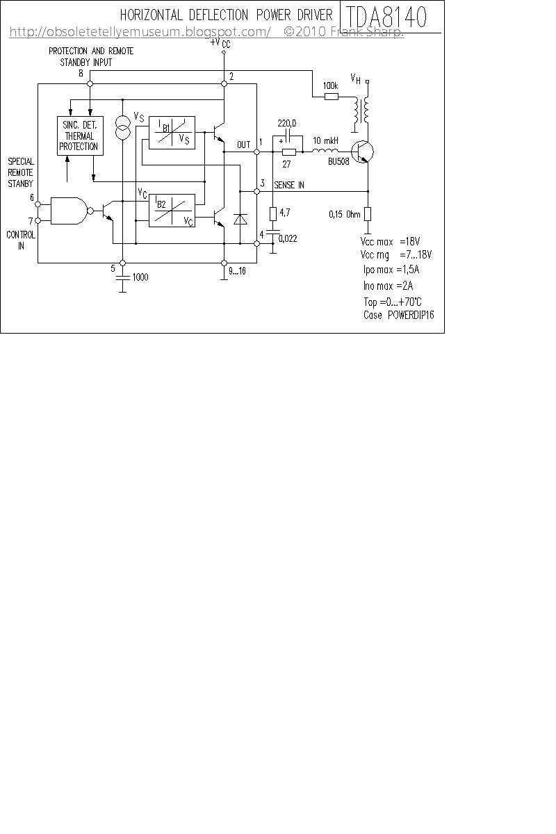 For the turn-OFF, the base of the power transistor
must be discharged by a quasi linear time decreasing
current as given in Figure 6.
Conventional driver systems inherently result into
a stable condition with a constant peak current
magnitude.
This is due to the constant base charge in the
turn-ON phase independent from the collector current
; hence a high peak current results into a low
storage time of the transistor because the excess
base charge is a minimum and vice versa. In the
active deflection the required function, high peak
current-fast switch-OFF and low peak current-slow
switch-OFF, is obtained by a controlled base discharge
current for the power transistor ; the negative
slope of this ramp is proportional to the actual
sensed current.
As a result, the active driving system even improves
the sharpnessof vertical lines on the screen
compared with the traditional solution due to the
increasedstability factor of the loop representedas
the variation of the storagetime versus the collector
peak current.
TDA4557 Multistandard decoder:
GENERAL DESCRIPTION
The TDA4557 is a monolithic integrated multistandard
colour decoder for the PAL, SECAM, NTSC 3.58 MHz and
NTSC 4.43 MHz standards.
FEATURES
Chrominance part
· Gain controlled chrominance amplifier for PAL, SECAM
and NTSC
· ACC rectifier circuits (PAL/NTSC, SECAM)
· Burst blanking (PAL) in front of 64 ms glass delay line
· Chrominance output stage for driving the 64 ms glass
delay line (PAL, SECAM)
· Limiter stages for direct and delayed SECAM signal
· SECAM permutator
Demodulator part
· Flyback blanking incorporated in the demodulators
(PAL, NTSC, SECAM)
· PAL switch
· Internal PAL matrix
· Two quadrature demodulators with external reference
tuned circuits (SECAM)
· Internal filtering of residual carrier
· De-emphasis (SECAM)
Identification part
· Automatic standard recognition by sequential inquiry
· Delay for colour-on and scanning-on
· Reliable SECAM identification by PAL priority circuit and
50/60 Hz recognition
· Forced switch-on of a standard
· Four switching voltages for chrominance filters, traps
and crystals
· Two identification circuits for PAL/SECAM (H/2) and
NTSC
· PAL/SECAM flip-flop
· SECAM identification mode switch (horizontal, vertical
or combined horizontal and vertical)
· Crystal oscillator with divider stages and PLL circuitry
(PAL, NTSC) for double colour subcarrier frequency
· HUE control (NTSC)
· Service switch
TDA8145 TV EAST/WEST CORRECTION CIRCUIT FOR SQUARE TUBES
FEATURES SUMMARY
■ LOW DISSIPATION
■ SQUARE GENERATOR FOR PARABOLIC
CURRENT SPECIALLY DESIGNED FOR
SQUARE C.R.T. CORRECTION
■ EXTERNAL KEYSTONE ADJUSTMENT
(symmetry of the parabola)
■ INPUT FOR DYNAMIC FIELD CO
RRECTION(beam current change)
■ STATIC PICTURE WIDTH ADJUSTMENT
■ PULSE-WIDTH MODULATOR
■ FINAL STAGE D-CLASS WITH ENERGY
REDELIVERY
■ PARASITIC PARABOLA SUPPRESSION,
DURING FLYBACK TIME OF THE VERTICAL
SAWTOOTH
DESCRIPTION
The TDA8145 is a monolithic integrated circuit in a
8 pin minidip plastic package designed for use in
the square C.R.T. east-west pin-cushion correction
by driving a diode modulator in TV and monitor
applications.
CIRCUIT OPERATION
(see the shematic diagram)
A differential amplifier OP1 is driven by a vertical
frequency sawtooth current of ± 33µA which is
produced via an external resistor fromthe sawtooth
voltage. The non–inverting input of this amplifier
is connected with a reference voltage
corresponding to the DC level of the sawtooth voltage.
This DC voltage should be adjustable for the
keystone correction. The rectified output current of
this amplifier drives the parabola networkwhich
provides a parabolic output current.
This output current produces the corresponding
voltage due to the voltage drop across the external
resistor at pin 7.
If the input is overmodulated (> 40µA) the internal
current is limited to 40µA. This limitation can be
used for suppressing the parasitic parabolic current
generated during the flyback time of the frame
sawtooth.
A comparator OP2 is driven by the parabolic current.
The second input of the comparator is connected
with a horizontal frequency sawtooth
voltage the DC level of which can be changed by
the external circuitry for the adjustment of the picture
width.
The horizontal frequency pulse–width modulated
output signal drives the final stage. It consists of a
class D push–pull output amplifier that drives, via
an external inductor, the diode modulator.
TDA2556 QUASI-SPLIT-SOUND CIRCUIT WITH DUAL SOUND DEMODULATORS
GENERAL DESCRIPTION
The TDA2556 is a monolithic integrated circuit for quasi-split-sound processing, including two FM
demodulators, for two carrier stereo TV receivers and VTR.
Features
First IF (vision carrier plus sound carrier).
0 3 stage gain controlled IF amplifier
0 AGC circuit
0 Reference amplifier and limiter amplifier for vision carrier (V.C.) processing
0 Linear multiplier for quadrature demodulation
Second IF (two separate channels for both FM sound signals).
0 4-stage-limiting amplifier
0 Ouadrature demodulator
0 AF amplifier with de-emphasis
O Output buffer
0 Muting for one or both AF outputs
No comments:
Post a Comment
The most important thing to remember about the Comment Rules is this:
The determination of whether any comment is in compliance is at the sole discretion of this blog’s owner.
Comments on this blog may be blocked or deleted at any time.
Fair people are getting fair reply. Spam and useless crap and filthy comments / scrapers / observations goes all directly to My Private HELL without even appearing in public !!!
The fact that a comment is permitted in no way constitutes an endorsement of any view expressed, fact alleged, or link provided in that comment by the administrator of this site.
This means that there may be a delay between the submission and the eventual appearance of your comment.
Requiring blog comments to obey well-defined rules does not infringe on the free speech of commenters.
Resisting the tide of post-modernity may be difficult, but I will attempt it anyway.
Your choice.........Live or DIE.
That indeed is where your liberty lies.
Note: Only a member of this blog may post a comment.